
Imaging device and camera

Inactive Publication Date: 2019-12-12
CANON KK
View PDF0 Cites 4 Cited by
  • Summary
  • Abstract
  • Description
  • Claims
  • Application Information

AI Technical Summary

Benefits of technology

The present invention provides an amplification circuit for an imaging device that can increase the ratio of minimum to maximum gain without increasing the physical size of the feedback capacitance. This is achieved by selectively setting the input and feedback capacitances based on their values, which in turn determines the gain of the amplification circuit. The resulting amplified pixel signal is converted into a digital signal using an A / D conversion circuit which uses a reference signal for comparison. The change rate per unit-time of the reference signal is smaller when the amplification circuit has a minimum gain, indicating a smaller impact on the signal-to-noise ratio. The technical benefits of this invention include improved amplification efficiency and reduced noise impact on the image quality.

Problems solved by technology

However, increasing the physical size of the feedback capacitance leads to an increase in chip size.
Also, reducing the physical size of the input capacitance faces limitations on miniaturization, and also leads to an increase in the effect of parasitic capacitance.

Method used


Image

  • Imaging device and camera
  • Imaging device and camera
  • Imaging device and camera

Examples


Embodiment Construction

[0010]Embodiments of the invention are described below with reference to the drawings. Like elements are denoted with the same reference numerals throughout the various embodiments, and redundant descriptions thereof are omitted. Further, the embodiments may be modified and combined as appropriate.

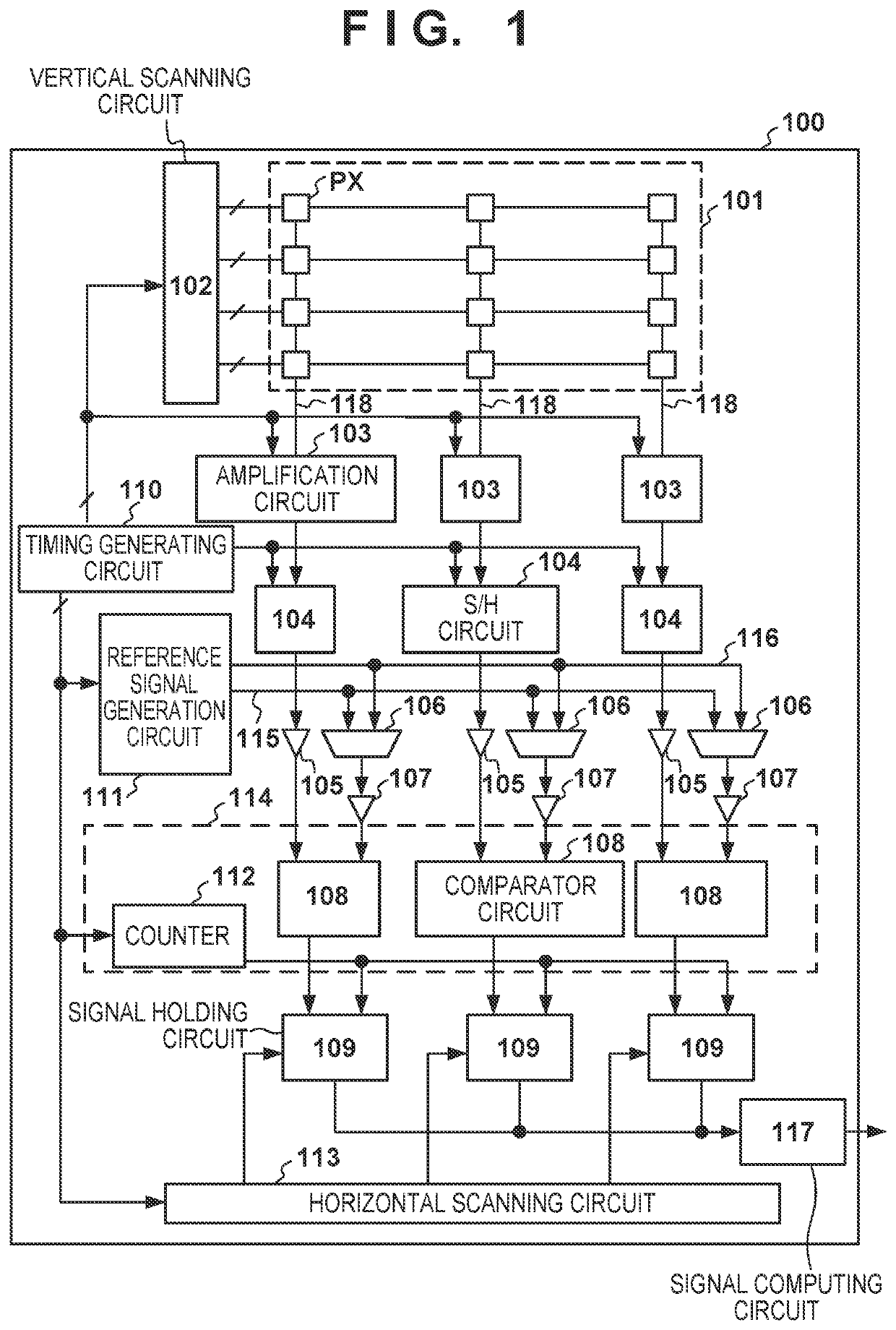
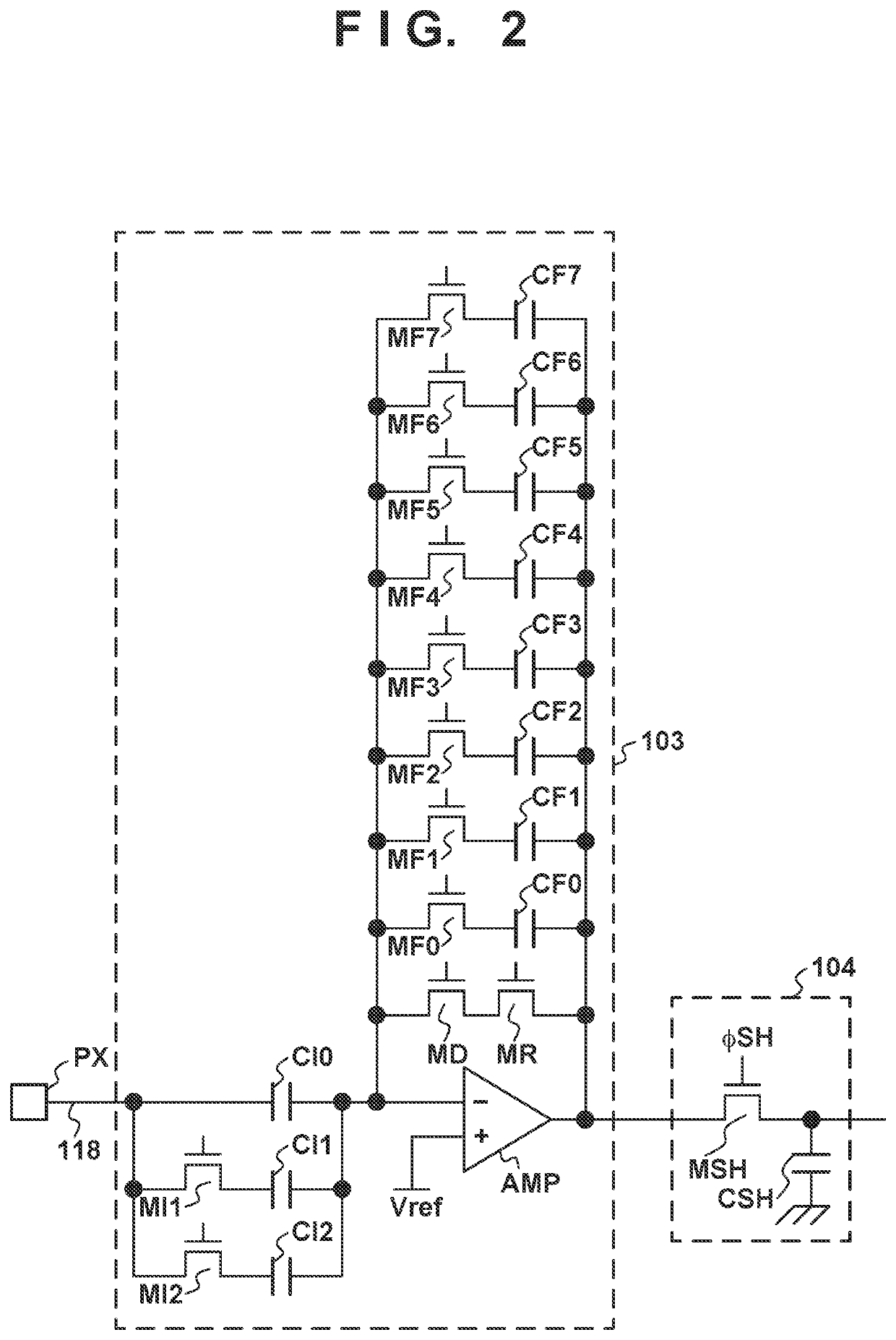
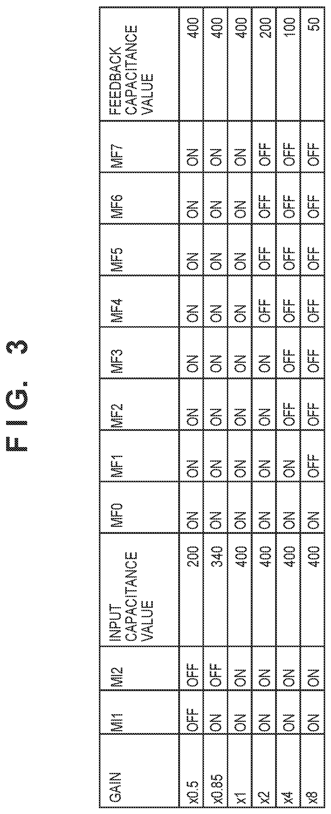
[0011]An overall configuration of an imaging device 100 according to some embodiments is described with reference to FIG. 1. The imaging device 100 includes the components illustrated in FIG. 1. The pixel array 101 is composed of a plurality of pixel circuits PX arranged in a matrix. Each pixel circuit PX generates an analog signal in accordance with the quantity of incident light. A vertical scanning circuit 102 sequentially selects each row of the pixel array 101. The analog signals for each pixel circuit PX included in the selected row are read to an amplification circuit 103 corresponding to each column of the pixel array 101. The analog signal generated in the pixel circuit PX include...


PUM


Abstract

An imaging device includes a pixel circuit, an amplification circuit, a control circuit, and an A / D conversion circuit. A value of the input capacitance of the amplification circuit is selectable from input capacitance values. A value of the feedback capacitance of the amplification circuit is selectable from feedback capacitance values. The control circuit sets the gain of the amplification circuit to be first through third gains by setting the value of the input capacitance and the value of the feedback capacitance. The A / D conversion circuit is of a voltage slope comparison type using a reference signal. A change rate per unit-time of the reference signal of a case where the amplification circuit has a minimum gain is smaller than a time change rate of the reference signal of a case where the amplification circuit has a maximum gain.

Description

BACKGROUND OF THE INVENTIONField of the Invention[0001]The present invention relates to an imaging device and a camera.Description of the Related Art[0002]An imaging device in which an amplification circuit is provided for each column of pixels is known. Japanese Patent Laid-Open No. 2002-198754 proposes the change of gain by switching the value of the input capacitance of the amplification circuit.SUMMARY OF THE INVENTION[0003]In the amplification circuit disclosed in Japanese Patent Laid-Open No. 2002-198754, a plurality of input capacitances are provided, while only a single feedback capacitance is provided. To increase the ratio (gain ratio) of the minimum gain to the maximum gain in the amplification circuit, the physical size of the feedback capacitance is required to be increased or the physical size of the input capacitance is required to be reduced. However, increasing the physical size of the feedback capacitance leads to an increase in chip size. Also, reducing the physic...

Claims


Application Information

Patent Timeline
IPC IPC(8): H04N5/3745H04N5/341H01L27/146H04N5/355
CPCH04N5/3559H01L27/14603H04N5/37455H04N5/341H04N25/75H04N25/772H04N25/40H04N25/59
Inventor AKABORI, HIROO
Owner CANON KK
Learn More