Semiconductor device and method for testing the same

Active Publication Date: 2011-09-22
SK HYNIX INC
View PDF4 Cites 7 Cited by
  • Summary
  • Abstract
  • Description
  • Claims
  • Application Information

AI Technical Summary

Benefits of technology

First, an embodiment of the present invention relates to a semiconductor device that allows a pair of bit lines to be equalized to a ground voltage level during a test mode, and simultaneously applies stress caused by the passing gate effect and stress caused by the neighbor gate effect to one cell during the test mode, thereby increasing the screen effect.
Second, an embodiment of the present invention relates to a semiconductor device that controls an even word line and an odd word line to be simultaneously enabled during the test mode, so that it can simultaneously tes

Problems solved by technology

However, in the case of using vertical-type cell transistors, capacitance between word lines is increased, resulting in a defective cell or failed cell operation.
However, failed parts (also called a fail phenomenon) caused by the neighbor gate operation have been increasingly generated in the sub 100 nm technology that uses a recess gate.
The fail phenomenon is becoming severe as the level of integration continues to increase.
Since a channel region is located below a junction region, cell function under a small critical dimension is unavoidably deteriorated due to the field influence caused by proximity with a neighbor passing gate or a neighbor gate.
Such deterioration may immediately lead to a fail of the off-leakage current, so that serious quality problems such as a March Cache OFF and the like may occur in a packaging step and a modularizing step.
In this way, if the threshold voltage of the cell transis

Method used


Image

  • Semiconductor device and method for testing the same
  • Semiconductor device and method for testing the same
  • Semiconductor device and method for testing the same

Examples


Example

Reference will now be made in detail to the embodiments of the present invention, examples of which are illustrated in the accompanying drawings. Wherever possible, the same reference numbers will be used throughout the drawings to refer to the same or like parts.

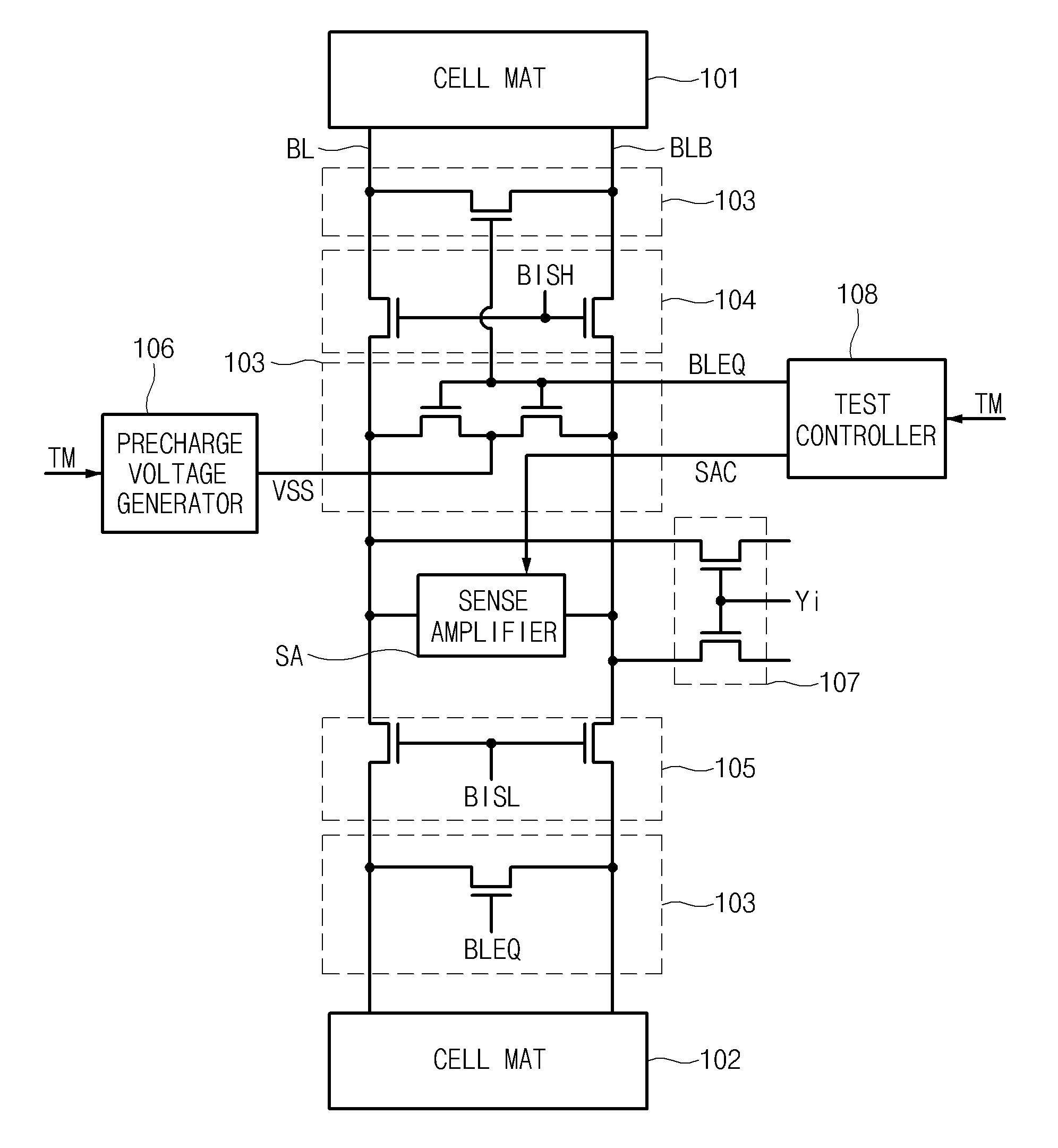
FIG. 4 is a circuit diagram illustrating a semiconductor device according to an embodiment of the present invention.

Referring to FIG. 4, a semiconductor device according to the present invention includes cell mats 101 and 102, a bit line precharge unit 130, switching units 104 and 105, a precharge voltage generator 106, a sense amplifier (SA), an output unit 107, and a test controller 108. In the embodiment shown in FIG. 4, two cell mats 101 and 102 are configured to share one sense amplifier SA. The cell mats 101 and 102 includes a memory cell.

A memory device, for example, the cell mats 101 and 102 of a DRAM, includes a plurality of bit lines and a plurality of word lines. In this case, the bit lines are arranged perpendic...


PUM


Abstract

A semiconductor device and a method for testing the same are disclosed, relating to a technology for simultaneously screening an off-leakage-current fail caused by a passing gate effect and a neighbor gate effect. The semiconductor device includes a memory cell configured to read and write data; a sense amplifier configured to sense and amplify cell data received from the memory cell through a pair of bit lines; a bit line precharge unit configured to equalize the pair of bit lines to a level of a ground voltage in response to a bit line equalization signal; a precharge voltage generator configured to provide the ground voltage to the bit line precharge unit during a test mode; and a test controller configured to, during the test mode, maintain an activation state of the bit line equalization signal during a test mode period, and control the sense amplifier to be deactivated.

Description

CROSS-REFERENCE TO RELATED APPLICATIONThe priority of Korean patent application No. 10-2010-0025341 filed on Mar. 22, 2010, the disclosure of which is hereby incorporated in its entirety by reference, is claimed.BACKGROUND OF THE INVENTIONEmbodiments of the present invention relate to a semiconductor device and a method for testing the same, and more specifically, to a technology for simultaneously screening an off-leakage-current fail caused by a passing gate effect and a neighbor gate effect.In recent times, vertical-type cell transistors have been rapidly introduced to the market due to the increasing level of integration. However, in the case of using vertical-type cell transistors, capacitance between word lines is increased, resulting in a defective cell or failed cell operation. The number of defective or failed cells is rapidly increased with the increasing level of integration.In a manufactured product of 100 nm or more that uses a cell transistor as a planar gate, a failed...

Claims


Application Information

Patent Timeline
IPC IPC(8): G11C29/00
CPCG11C29/12005G11C2029/5006G11C2029/1204G11C29/50
Inventor LEE, WON HEE
Owner SK HYNIX INC
Why Eureka
Try Eureka