Integrated circuit (IC) design systems and methods using single-pin imaginary devices

a technology of integrated circuits and imaginary devices, applied in cad techniques, special data processing applications, instruments, etc., can solve problems such as unnecessary area for performance trade-offs, unnecessary area consumption, and unnecessarily limit size scaling

Active Publication Date: 2019-12-19
MARVELL ASIA PTE LTD
View PDF0 Cites 1 Cited by
  • Summary
  • Abstract
  • Description
  • Claims
  • Application Information

AI Technical Summary

Benefits of technology

[0009]It should be noted that other design method embodiments could similarly use single-pin imaginary devices in a schematic diagram for the purpose of identifying one or more groups of components and also group-aware design rules during design layout generation. Specifically, an embodiment of a design method can include accessing, from a memory, a schematic diagram that depicts components of an IC and, connected to at least two of the components, single-pin imaginary devices that are associated with group properties of the components. That is, some components in the IC can be assigned to groups (e.g., based on a common feature). In the schematic diagram, each component that is assigned to a specific group can be connected to a single-pin imaginary device, which is a...

Problems solved by technology

Oftentimes, however, the design rules of a specific technology node will be overly pessimistic (i.e., enforced based on the assumption of worst-case conditions) and this pessimism can result in unnecessary area for performance trade-offs.
However, considering that in a given IC design, some...

Method used


Image

  • Integrated circuit (IC) design systems and methods using single-pin imaginary devices
  • Integrated circuit (IC) design systems and methods using single-pin imaginary devices
  • Integrated circuit (IC) design systems and methods using single-pin imaginary devices

Examples


Embodiment Construction

[0021]As mentioned above, oftentimes the design rules of a specific technology node will be overly pessimistic (i.e., enforced based the assumption of worst-case conditions) and this pessimism can result in unnecessary area for performance trade-offs.

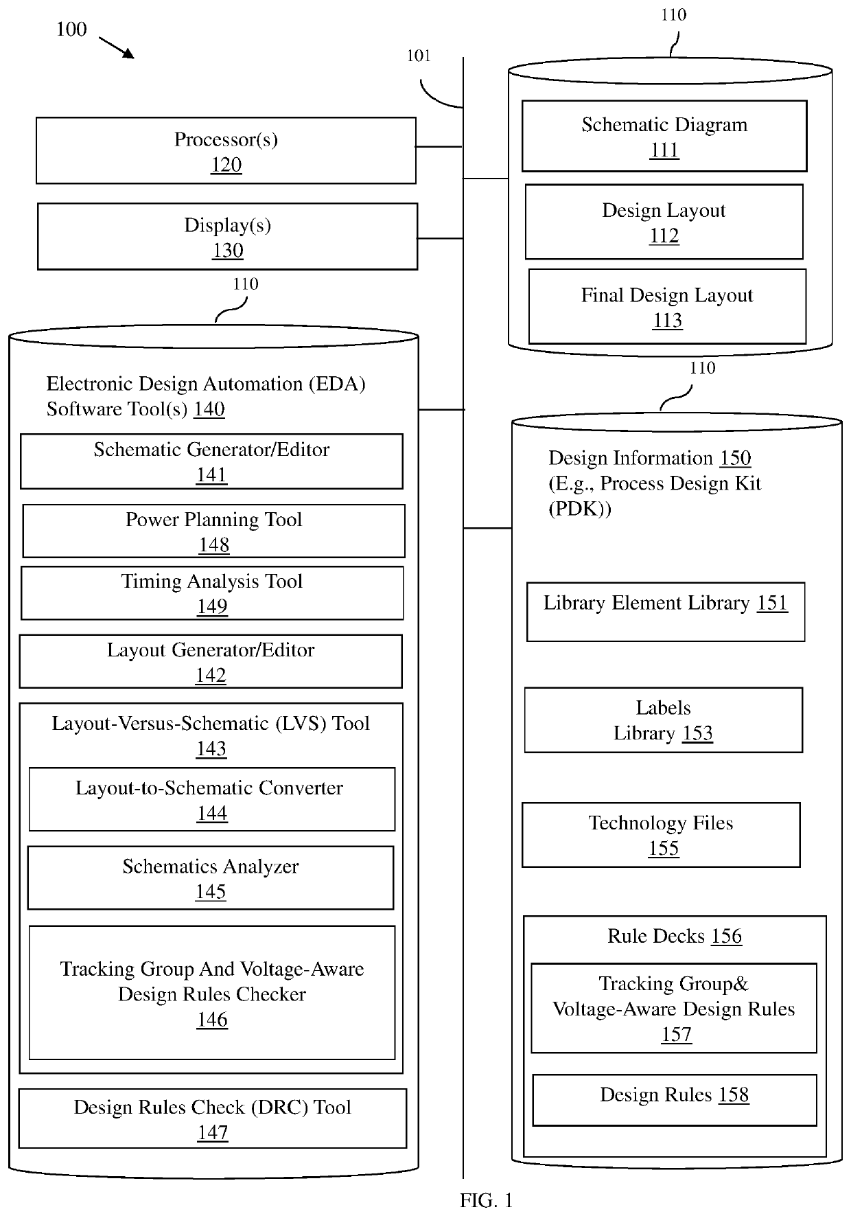
[0022]In view of the foregoing, disclosed herein are embodiments of computer-aided integrated circuit (IC) design systems and methods. In the embodiments, some circuit components have common features that can be noted within the IC schematic diagram using single-pin imaginary devices so that these common features can be considered during the design flow to, for example, minimize area consumption and improve IC reliability.

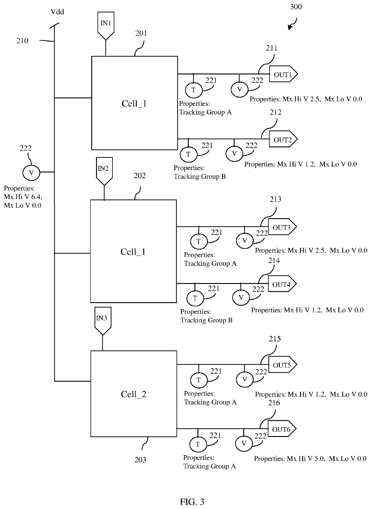
[0023]For purposes of this disclosure, an “imaginary device” in a schematic diagram is device symbol that is not representative of an actual device within the IC (i.e., a device that is to be manufactured), but instead is inserted into the schematic diagram and employed in order to provide additional, circuit-specific ...


PUM


Abstract

In the disclosed design systems and methods, a schematic diagram includes nets and, connected to at least some nets, single-pin first and second imaginary devices. On any given net, a first imaginary device is associated with a tracking group property of the net (where nets in the same tracking group are in-phase) and a second imaginary device is associated with a voltage property of the net. A design layout generated based on the schematic diagram includes: net shapes representing the nets and, on net shapes that represent nets connected to the imaginary devices, tracking group and voltage labels corresponding to the tracking group and voltage properties. Net shape placement within the design layout and design rule checking are performed according to design rules that dictate placing net shapes with the same tracking group label together and further dictate minimum allowable spacing requirements depending upon the tracking group and voltage labels.

Description

BACKGROUNDField of the Invention[0001]The present invention relates to area-optimized integrated circuit (IC) design and, particularly, to computer-aided design (CAD) systems and methods that enable IC components with common features (e.g., nets that are in-phase, also referred to as tracking nets) to be identified and considered during the design flow, particularly, during IC design layout generation (e.g., for area-optimization) and layout verification (e.g., for chip reliability).Description of Related Art[0002]In integrated circuit (IC) design, a schematic-driven layout (SDL) tool is a computer-aided design (CAD) tool that analyzes a schematic diagram of an IC and, based on the information contained in that schematic diagram and further based on a set of design rules for a particular technology node at issue, generates a design layout for the IC. The design layout generated by the SDL tool will subsequently undergo physical verification, which includes, but is not limited to: la...

Claims


Application Information

Patent Timeline
IPC IPC(8): G06F17/50
CPCG06F2217/12G06F17/5081G06F2217/06G06F2217/02G06F30/392G06F30/394G06F30/398G06F2111/04G06F2111/20G06F2119/18
Inventor LAU, HENG LANPRABHU, MANJUNATHACHAUHAN, VIKRANT KUMARWALSH, SHAWN
Owner MARVELL ASIA PTE LTD
Why Eureka
Try Eureka