Package architecture with improved via drill process and method for forming such package

a technology of packaging and vias, applied in semiconductor devices, semiconductor/solid-state device details, electrical devices, etc., can solve problems such as easy ablation, void vias and/or underfilled vias, and plating defects

Active Publication Date: 2019-12-26
INTEL CORP
View PDF0 Cites 4 Cited by
  • Summary
  • Abstract
  • Description
  • Claims
  • Application Information

AI Technical Summary

Problems solved by technology

This may lead to several problems including voided vias and / or underfilled vias caused by undercuts (or voids) formed in the metal pad as a result of the lasers' ablation.
As such, this laser ablation may result in plating defects which may potentially appear as unfilled vias in the final semiconductor package / product.
This AP layer, however, may also be easily ablated and does not protect the metal pad from high energy laser sources.
These available packaging solutions limit the laser power and thus rely on reducing the incoming energy on to the dielectric and / or the surface of the metal pad.
In each of these cases, nonetheless, there are significant challenges with delivering a manufacturable BMV drill process for the next generation FLS semiconductor packages, including increased cost, uncertainty, and complexity.
In addition, these packaging solutions reduce the efficacy of the laser drill process by limiting the use of such powerful and accurate lasers used for rapidly creating high resolution BMVs.
These limitations not only limit the BMV processing options but also delay the adoption of next generation packaging architectures.

Method used


Image

  • Package architecture with improved via drill process and method for forming such package
  • Package architecture with improved via drill process and method for forming such package
  • Package architecture with improved via drill process and method for forming such package

Examples


example 17

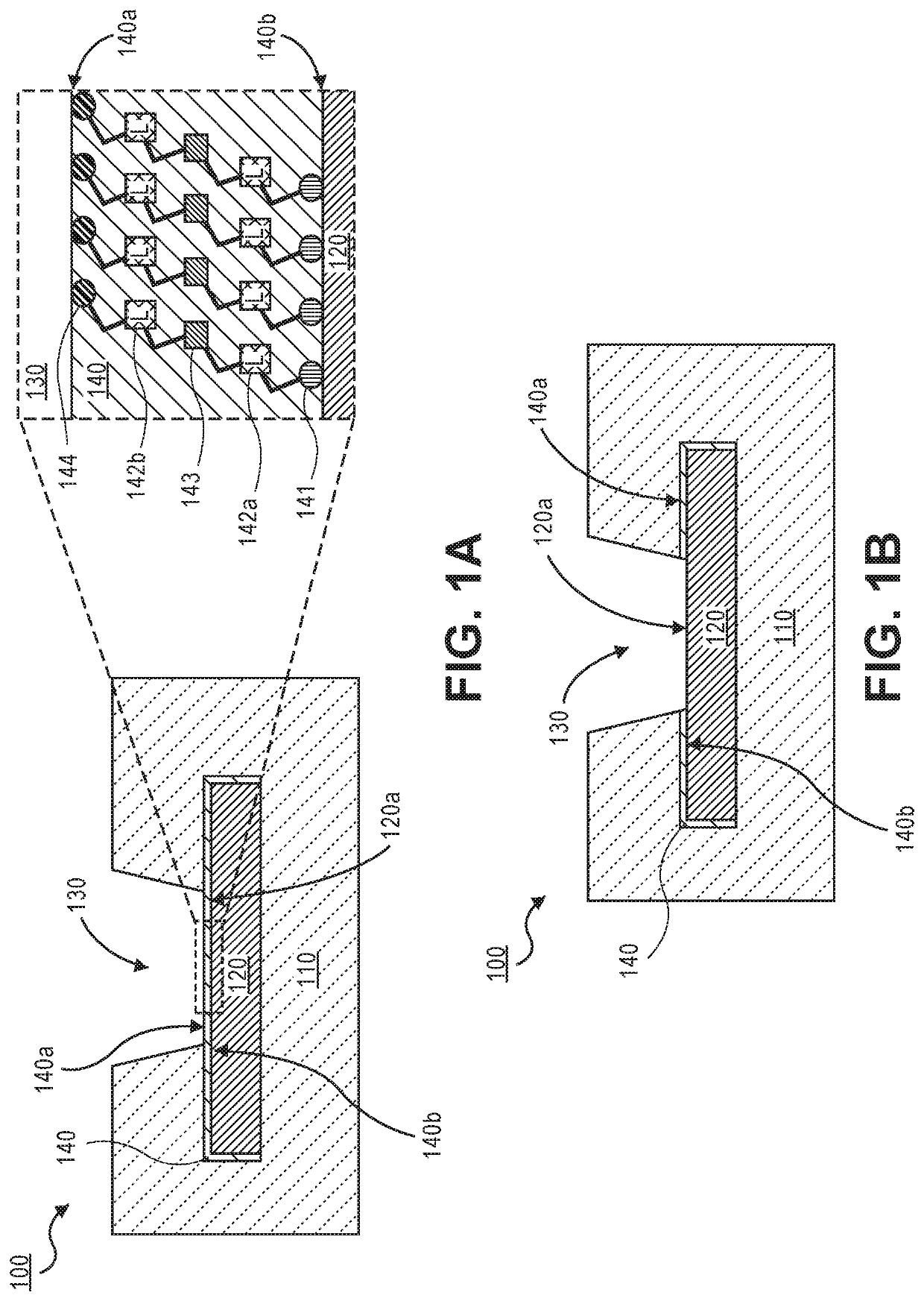
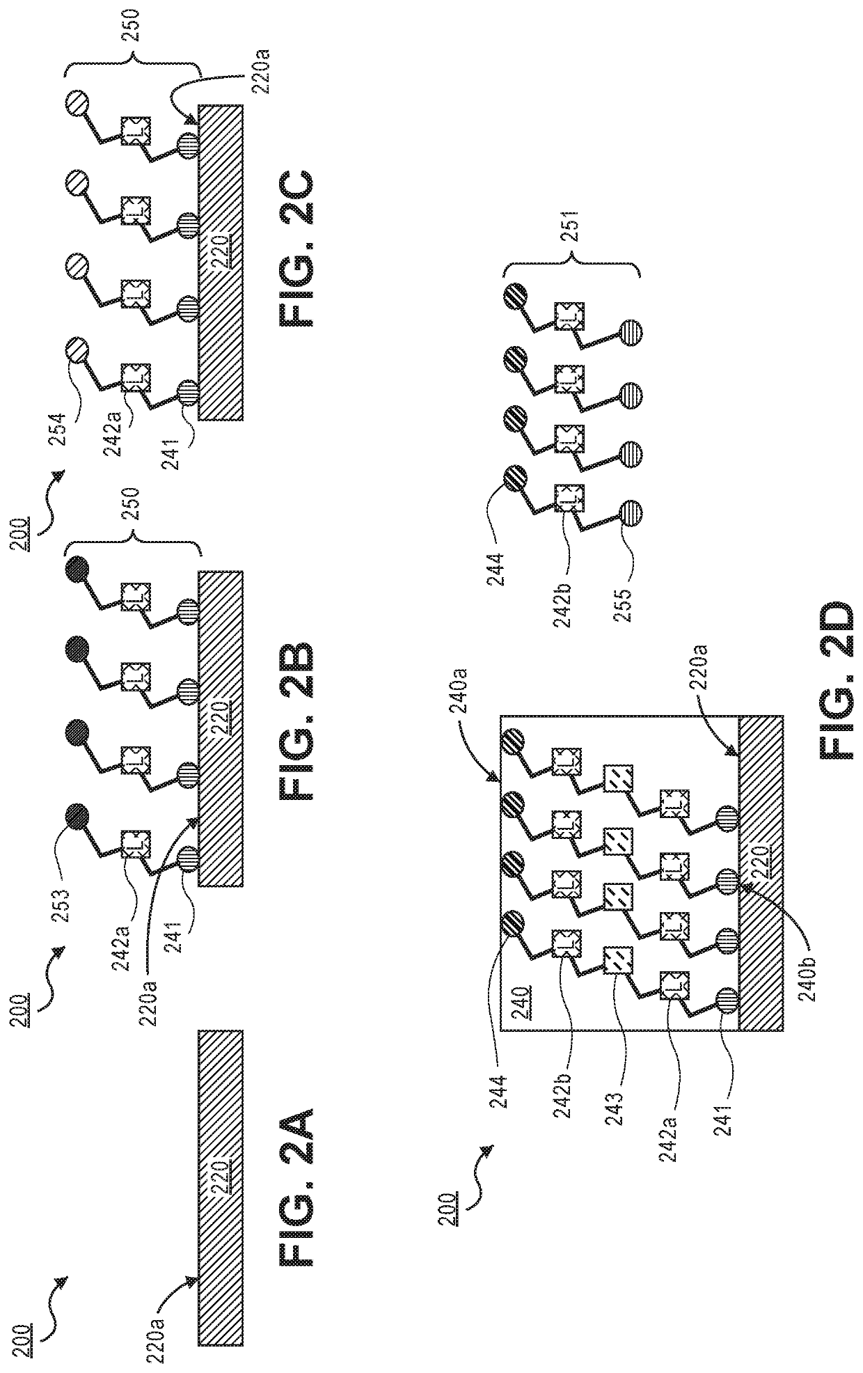
[0124 is an organic layer comprising of a first monolayer having a first end group and at least one of a second end group and a third end group; a second monolayer having a fourth end group and a fifth end group. The first monolayer and the second monolayer include at least one of a first plurality of light-reflective moieties and a second plurality of light-reflective moieties; and an intermediate group bonding the fourth end group of the second monolayer and at least one of the second end group and the third end group of the first monolayer to form a SAM layer. The intermediate group includes at least one of a first reactive bond of the second end group and the fourth end group and a second reactive bond of the third end group and the fourth end group.

[0125]In example 18, the subject matter of example 17 can optionally include the SAM layer which includes a molecular structure having the first end group, the intermediate group, the fifth end group, and at least one of the first pl...


PUM


Abstract

Embodiments include a package substrate, a method of forming the package substrate, and a self-assembled monolayers (SAM) layer. The package substrate includes a SAM layer on portions of a conductive pad, where the SAM layer includes alight-reflective moieties. The package substrate also includes a via on a surface portion of the conductive pad, and a dielectric on and around the via, the SAM layer, and the conductive pad, where the SAM layer surrounds and contacts a surface of the via. The SAM layer may be an interfacial organic layer. The light-reflective moieties may include a hemicyanine, a cyclic-hemicyanine, an oligothiophene, and / or a conjugated aromatic compound. The SAM layer may include a molecular structure having a first end group of a first monolayer, an intermediate group, a fifth end group of a second monolayer, and one or more of a first and second light-reflective moieties.

Description

FIELD[0001]Embodiments relate to packaging semiconductor devices. More particularly, the embodiments relate to a package substrate having an organic self-assembled monolayers (SAM) layer with light-reflecting moieties and methods for forming such package substrate.BACKGROUND[0002]Substrates for next generation chip-to-chip interconnect technologies require significantly higher speed and higher density input / output (IO) routing. Next generation packaging solutions are trending to higher I / O densities to meet the rapidly increasing demand for greater connectivity and faster speeds. To meet this increasing demand, the semiconductor packaging roadmap is pressed to deliver a smaller blind micro vias (BMVs) and a rapidly decreasing fine line spacing (FLS) requirement, for example, from the existing FLS requirement of roughly 9 / 12 μm towards 2 / 2 μm or less.[0003]Ultra-violet (UV) lasers are typically used to form such BMVs, while excimer based lasers may be used for next generation package...

Claims


Application Information

Patent Timeline
Patent Type & Authority Applications(United States)
IPC IPC(8): H01L23/00H01L23/29H01L21/48H01L21/56
CPCH01L21/563H01L24/17H01L21/486H01L24/33H01L23/293H01L24/27H01L24/11H01L23/5329H01L21/4857H01L23/49822H01L24/16H01L24/29H01L24/32H01L24/73H01L2224/131H01L2224/13101H01L2224/13111H01L2224/13147H01L2224/13155H01L2224/13164H01L2224/16225H01L2224/2919H01L2224/32225H01L2224/73204H01L2224/81801H01L2224/83851H01L2924/15311H01L2924/00012H01L2924/014H01L2924/00014H01L2924/013H01L2924/01028H01L2924/01046H01L2924/0105
Inventor NAD, SUDDHASATTWAMANEPALLI, RAHULWALL, MARCEL
Owner INTEL CORP
Why Eureka
Try Eureka