Semiconductor device

a technology of semiconductors and devices, applied in the direction of transistors, electronic switching, pulse techniques, etc., can solve the problems that the logical circuit may not achieve the desired specifications, and achieve the effect of reducing the variation of electrical characteristics

Active Publication Date: 2019-12-26
SOCIONEXT INC
View PDF0 Cites 0 Cited by
  • Summary
  • Abstract
  • Description
  • Claims
  • Application Information

AI Technical Summary

Benefits of technology

[0006]The embodiments of the present disclosure provide a semiconductor device including a logical circuit so as to decrease its variations of electrical characteristics.

Problems solved by technology

However, the logical circuit in proximity of the power switching circuit may have variations of electrical characteristics, and thus the logical circuit may fail to achieve desired specifications.

Method used


Image

  • Semiconductor device
  • Semiconductor device
  • Semiconductor device

Examples


first embodiment

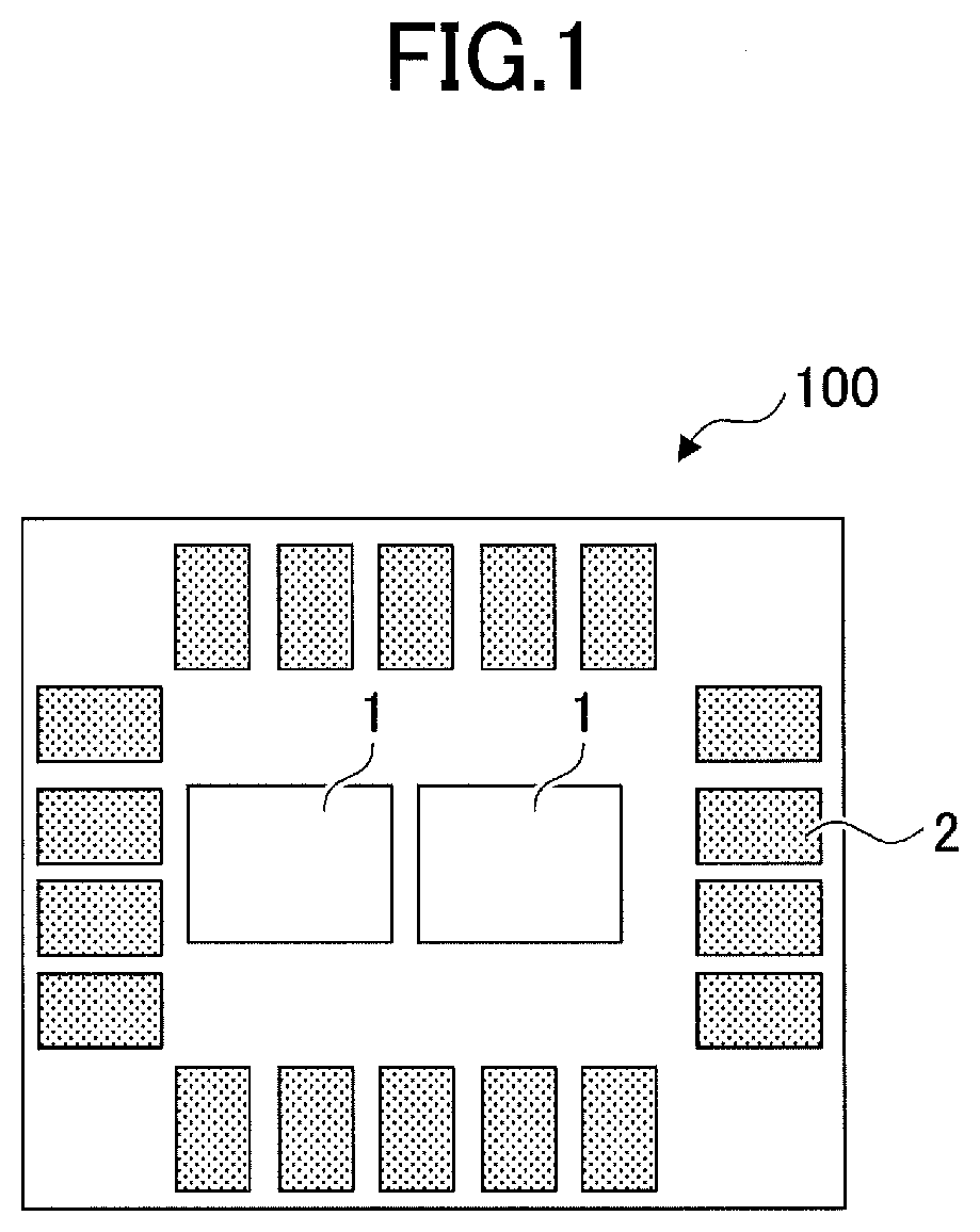
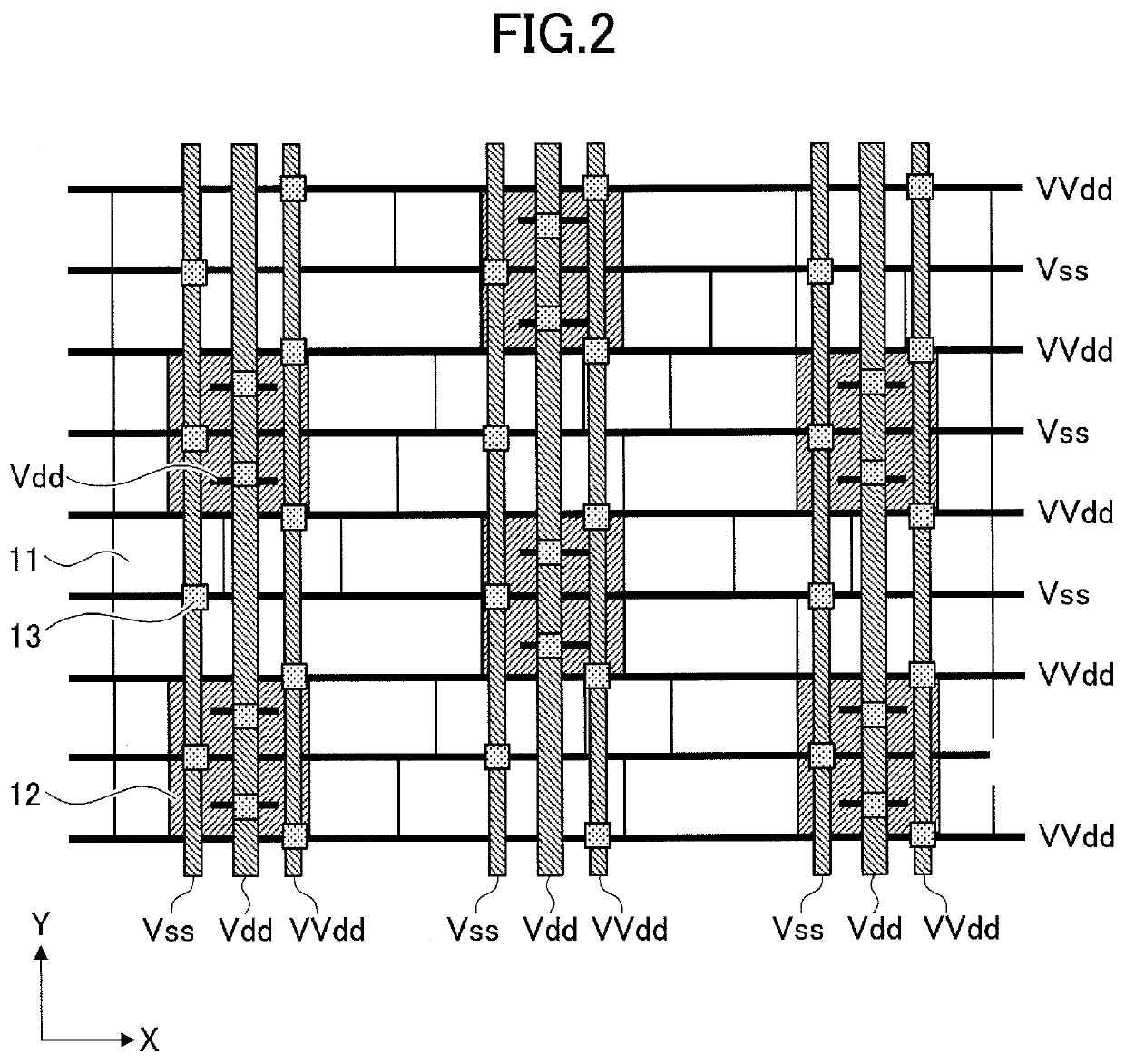
[0037]A first embodiment is described hereafter. FIG. 1 is a diagram illustrating an example of a layout of a semiconductor device according to a first embodiment. FIG. 2 is a diagram illustrating an example of an enlargement of part of a standard cell region.

[0038]As illustrated in FIG. 1, a semiconductor device 100 according to the first embodiment includes a plurality of standard cell regions 1, and input and output (I / O) cell regions 2 around the standard cell regions 1. As illustrated in FIG. 2, in the standard cell region 1, a plurality of standard cells 11 and a plurality of power switching circuits 12 are arranged. The standard cells 11 each include various logical circuits such as a NAND circuit and an inverter circuit. In the standard cell region 1, Vss interconnects for supplying a ground potential to the standard cells 11, as well as VVdd interconnects for supplying a power supply potential to the standard cells 11, are arranged. In the present embodiment, a Vss intercon...

second embodiment

[0084]A second embodiment is described hereafter. The second embodiment differs from the first embodiment in terms of the arrangement of the region RBU2 for a buffer BU2. FIG. 13 is a diagram illustrating, in a plan view, an example of a configuration of a well according to the second embodiment. FIG. 14 is a diagram illustrating, in a plan view, an example of a relationship between active regions and an element isolation region according to the second embodiment. FIG. 15 is a diagram illustrating, in a plan view, an example of a configuration of fins, gate electrodes and local interconnects according to the second embodiment. FIG. 16 is a diagram illustrating, in a plan view, an example of a relationship with respect to a first interconnect layer, the gate electrodes and the local interconnects according to the second embodiment. FIG. 17 is a diagram illustrating, in a plan view, an example of a relationship between a second interconnect layer and the first interconnect layer accor...

third embodiment

[0095]A third embodiment is described hereafter. The third embodiment differs from the second embodiment in terms of the arrangement of the active regions ASW21 and ASW22 included in the region RSW2. FIG. 19 is a diagram illustrating, in a plan view, an example of a configuration of fins, gate electrodes and local interconnects according to the third embodiment. FIG. 20 is a diagram illustrating, in a plan view, an example of a relationship with respect to a first interconnect layer, the gate electrodes and the local interconnects according to the third embodiment. FIG. 21 is a diagram illustrating, in a plan view, an example of a relationship between a second interconnect layer and the first interconnect layer according to the third embodiment. FIG. 22 is a cross-sectional view illustrating an example of a configuration of a semiconductor device according to the third embodiment. FIG. 22 is a cross-sectional view taken along line I-I in FIGS. 19 to 21. FIGS. 19 to 21 illustrate an ...


PUM


Abstract

A semiconductor device includes a semiconductor substrate, a first standard cell including a first active region and a second active region, and a power switching circuit including a first switching transistor electrically connected between a first interconnect and a second interconnect over the semiconductor substrate, and including a first buffer connected to a gate of the first switching transistor, the first buffer including a third active region and a fourth active region, and wherein the first buffer adjoins, in a plan view, the first standard cell in a first direction, wherein an arrangement of the first active region matches an arrangement of the third active region in a second direction different from the first direction, and wherein an arrangement of the second active region matches an arrangement of the fourth active region in the second direction.

Description

CROSS-REFERENCE TO RELATED APPLICATION[0001]This application is based upon and claims the benefit of priority of the Japanese Patent Application No. 2018-119819, filed on Jun. 25, 2018, the entire contents of which are incorporated herein by reference.BACKGROUND OF THE INVENTION1. Field of the Invention[0002]The present disclosure relates to a semiconductor device.2. Description of the Related Art[0003]A semiconductor device includes various circuit regions, and a standard cell region is used as a circuit region by way of example. In such a standard cell region, various logical circuits and power switching circuits are arranged.[0004]For example, a power switching circuit is disposed between a power supply interconnect with supplied Vdd potential and an interconnect for supplying VVdd power to transistors in logical circuits. The VVdd power to the transistors is switched on or off by the power switching circuit. With use of the power switching circuit, power supply is switched off w...

Claims


Application Information

Patent Timeline
Patent Type & Authority Applications(United States)
IPC IPC(8): H01L27/02H01L27/092H01L23/522H01L23/528H01L29/78H01L29/06
CPCH01L29/0696H01L27/0207H01L23/5283H01L23/5226H01L29/7851H01L27/0928H03K17/687H03K19/094H01L27/092H01L27/0924H01L27/11807H01L27/11898H01L21/76895H01L23/528
Inventor WANG, WENZHENTAKENO, HIROTAKAOKAMOTO, ATSUSHI
Owner SOCIONEXT INC
Why Eureka
Try Eureka