Light-detecting device and manufacturing method thereof

a technology of light-detecting devices and manufacturing methods, which is applied in the direction of sustainable manufacturing/processing, crystal growth process, final product manufacturing, etc., can solve the problems of distortion stress, distortion stress, and the inability to realize low-power solid-state image pickup devices, so as to improve the gettering effect and reduce the electric characteristic variation

Inactive Publication Date: 2007-09-06
PANASONIC CORP
View PDF6 Cites 1 Cited by
  • Summary
  • Abstract
  • Description
  • Claims
  • Application Information

AI Technical Summary

Benefits of technology

[0008]An object of the present invention is therefore to provide a light-detecting device for improving a gettering effect and reducing an electric characteristic variation, and a manufacturing method of the light-detecting device.

Problems solved by technology

This causes a distortion stress for getting a heavy-metal impurity and a crystal defect.
In addition, a distortion stress is caused because anatomic radius of each of silicon and carbon is different.
If an electric characteristic variation becomes larger among devices, a low-power solid-state image pickup device cannot be realized because various kinds of applied voltages are required to be higher.
Note that this problem occurs not only in a solid-state image pickup device but also in a light-detecting device to which a gettering technology is applied (such as light-receiving elements for photocoupler, optical communication, an optical pickup and the like).

Method used


Image

  • Light-detecting device and manufacturing method thereof
  • Light-detecting device and manufacturing method thereof
  • Light-detecting device and manufacturing method thereof

Examples


first embodiment

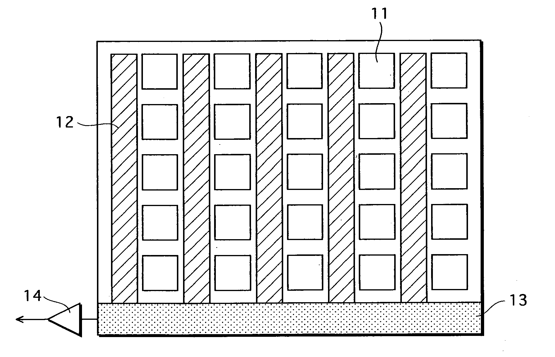
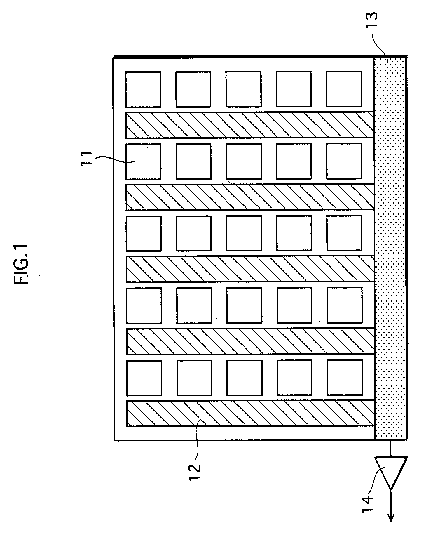
[0057]FIG. 1 shows a schematic construction of an IT-CCD type solid-state image pickup device.

[0058]The solid-state image pickup device includes a plurality of light-detecting units 11, a plurality of vertical transferring units 12, a horizontal transferring unit 13, and an amplifying unit 14.

[0059]The plurality of light-detecting units 11 are arranged in a matrix in a plane to generate charges corresponding to the amount of received light. The plurality of light-detecting units 11 for 25 pixels of 5 rows and 5 columns are shown in FIG. 1. Each of the plurality of vertical transferring units 12 transfers the charge generated by each of the plurality of light-detecting units 11 to the horizontal transferring unit 13. The horizontal transferring unit 13 transfers the charge from each of the plurality of vertical transferring units 12 to the amplifying unit 14. The amplifying unit 14 converts the charge from the horizontal transferring unit 13 into a voltage and outputs it.

[0060]FIG. 2...

second embodiment

[0118]FIG. 11 shows a schematic construction of a FT-CCD type solid-state image pickup device.

[0119]The solid-state image pickup device includes a light-receiving region 41, an accumulation region 42, a horizontal transferring unit 43, and an amplifying unit 46.

[0120]The light-receiving region 41 has a plurality of light-detecting units 44. Each of the plurality of light-detecting units 44 generates a charge corresponding to the amount of received light, and functions as a vertical transferring unit. The accumulation region 42 has a plurality of accumulation units 45. Each of the plurality of accumulation units 45 accumulates the charge transferred from each of the plurality of light-detecting units 44, and functions as a vertical transferring unit. The plurality of light-detecting units 44 and the plurality of accumulation units 45 are arranged in a matrix in a plane. Each of the plurality of light-detecting units 44 and the plurality of accumulation units 45 for 66 pixels of 6 row...

third embodiment

[0129]FIG. 13 is a cross section of a light-receiving element for photocoupler.

[0130]The light-receiving element includes a semiconductor substrate 401, an epitaxial layer 402, an insulating film 408, a transparent electrode 409, and an antireflection film 416.

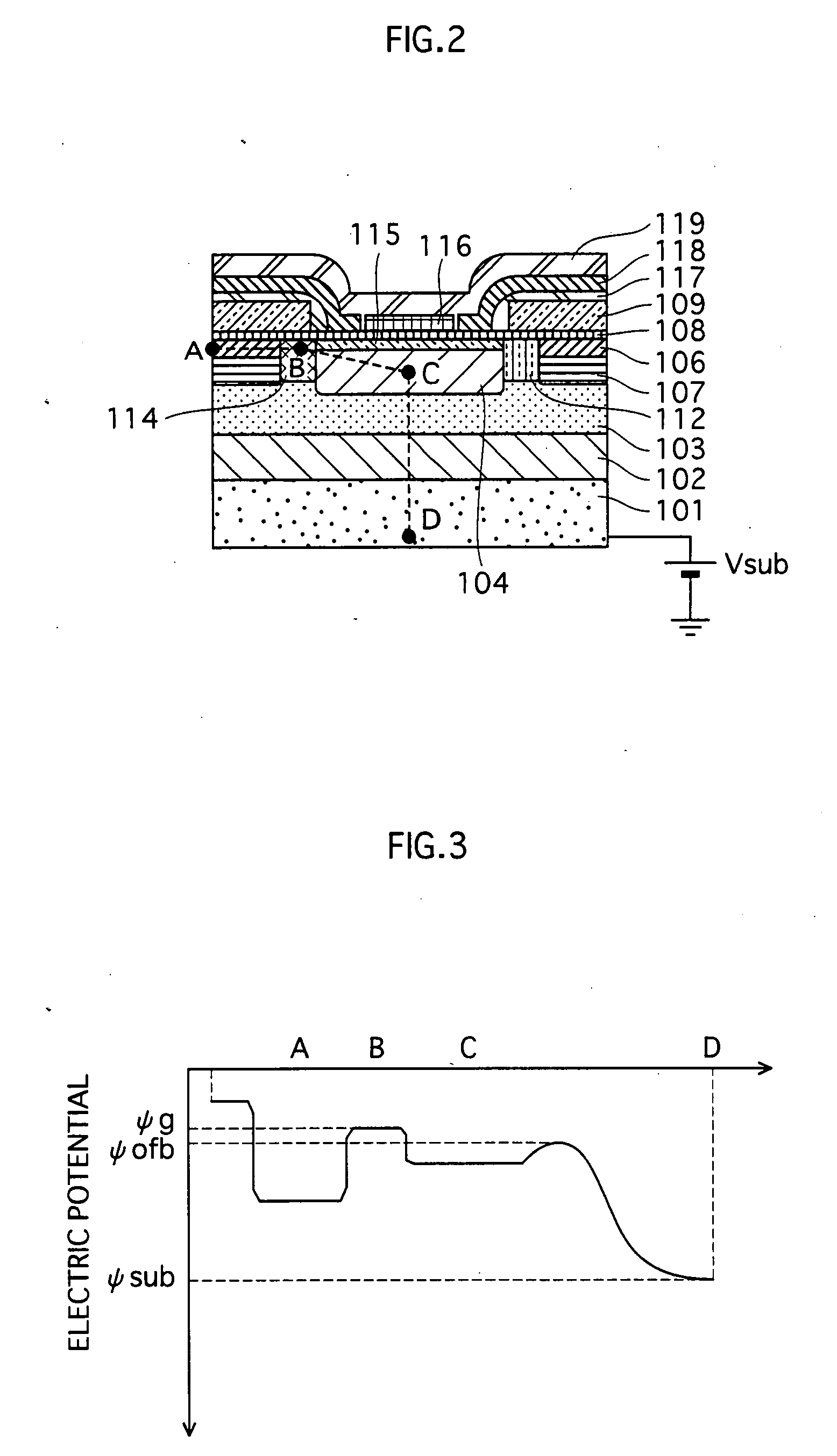
[0131]The semiconductor substrate 401 is composed of silicon as a base material and contains carbon and phosphorous. Carbon is substantially uniformly distributed in the semiconductor substrate 401 in a plane direction and a depth direction. A carbon concentration is in a range of 1×10¹⁶ atoms / cm3 to 2.5×10¹⁷ atoms / cm3 inclusive.

[0132]The epitaxial layer 402 includes a p-type well region 403 and a n-type region 404. The p-type well region 403 forms the overflow barrier electric potential ψofb between the n-type region 404 and the semiconductor substrate 401. A potential well is formed because the n-type region 404 is surrounded by the p-type well region 403. An area in which the potential well is formed corresponds to a light-...


PUM

PropertyMeasurementUnit
sizeaaaaaaaaaa
thicknessaaaaaaaaaa
temperatureaaaaaaaaaa

Abstract

A light-detecting device, comprising: a semiconductor substrate 101 that is composed of silicon as a base material, and contains carbon at a predetermined concentration; and an epitaxial layer 102 that is formed on the semiconductor substrate 101 and composed of silicon as a base material, the epitaxial layer 102 including a light-detecting unit (mainly 104) a predetermined distance away from the semiconductor substrate 101, wherein the semiconductor substrate 101 is formed using a crystal growth method from melt obtained by melting a material containing silicon and a material containing carbon so that carbon is contained in the semiconductor substrate 101 at the predetermined concentration.

Description

BACKGROUND OF THE INVENTION[0001](1) Field of the Invention[0002]The present invention relates to a light-detecting device and a manufacturing method thereof, and especially to a gettering technology.[0003](2) Description of the Related Art[0004]A gettering technology is generally applied to a solid-state image pickup device which is one type of light-detecting device, to reduce a white scratch and a dark current. The gettering technology is a technology for removing a heavy-metal impurity (Fe, Ni, and the like) and a crystal defect as main factors of a white scratch and the like from a device forming area of a semiconductor substrate. In IG (Intrinsic Gettering) as a typical gettering technology, a BMD ((Bulk Micro Defect) mainly an oxygen precipitation defect) is generated inside of a semiconductor substrate by performing a heat treatment. This causes a distortion stress for getting a heavy-metal impurity and a crystal defect. As a result, a heavy-metal impurity is removed from a ...

Claims


Application Information

Patent Timeline
Patent Type & Authority Applications(United States)
IPC IPC(8): H01L29/30
CPCC30B15/04C30B29/06H01L21/3221H01L27/14687H01L27/14843Y02E10/547H01L27/14887H01L31/03921H01L31/12H01L31/1804H01L27/1485Y02P70/50
Inventor HIRAI, JUNSUZUKI, MASAKATSUMURAKAMI, ICHIROHIROFUJI, YUICHI
Owner PANASONIC CORP
Why Eureka
Try Eureka