
Electronic component housing package and electronic component housing method

a technology of electronic components and electronic components, applied in the field can solve the problems of difficult to take out individual electronic components from the embossed recess, difficult to mount ultra-thin electronic components, difficult to house individual electronic components in a carrier tape for shipping, etc., to achieve the effect of preventing suction errors and easy production of electronic component housing packages

Pending Publication Date:
View PDF0 Cites 0 Cited by
  • Summary
  • Abstract
  • Description
  • Claims
  • Application Information

AI Technical Summary

Benefits of technology

The present invention allows for the efficient and shipping of ultra-thin electronic components. By using a carrier tape and a base film in which the adhesive film is placed, the adhesive film does not stick to the carrier tape during shipping. The electronic component can be easily removed by pushing it up through the base film. An adhesive layer may be added to stick the carrier tape and base film together, making it easy to position and remove the electronic component. The invention also allows for the separation of the adhesive film from the electronic component when needed. Overall, the invention allows for efficient and safe shipping of electronic components.

Problems solved by technology

Such an ultra-thin type electronic component is not easy to handle at mounting, so that it is sometimes shipped in a state of being stuck with an adhesive film such as a die attach film.
On the other hand, it is difficult to house individualized electronic components in a carrier tape for shipping.
That is, when the electronic components stuck with the adhesive film are housed in a normal carrier tape, the adhesive tape ends up sticking with the carrier tape, making it difficult to take out the individual electronic components from the embossed recess.
Particularly, when electronic components stuck with the adhesive film are of an ultra-thin type, they may be damaged when being peeled off from the carrier tape.
It can be considered to previously cover the surface of the adhesive film with a release layer so as to prevent the adhesive film and carrier tape from sticking to each other; in this case, however, the electronic component may move inside the embossed recesses, which poses a new problem of occurrence of suction error when the electronic component is taken out using a pickup tool.

Method used


Image

  • Electronic component housing package and electronic component housing method
  • Electronic component housing package and electronic component housing method
  • Electronic component housing package and electronic component housing method

Examples


first embodiment

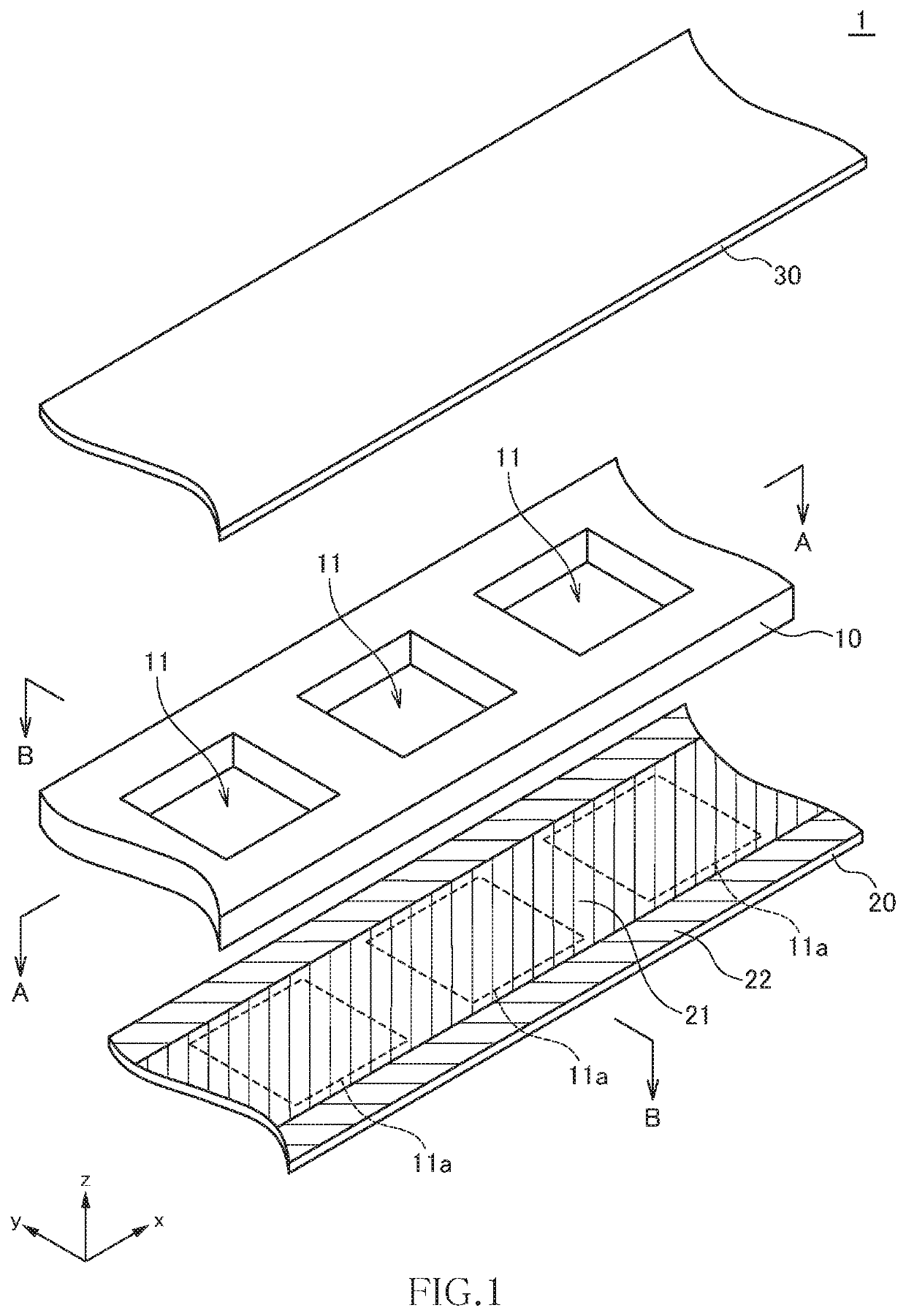
[0036]FIG. 1 is a schematic exploded perspective view for explaining the configuration of an electronic component housing package 1 according to the first embodiment of the present invention.

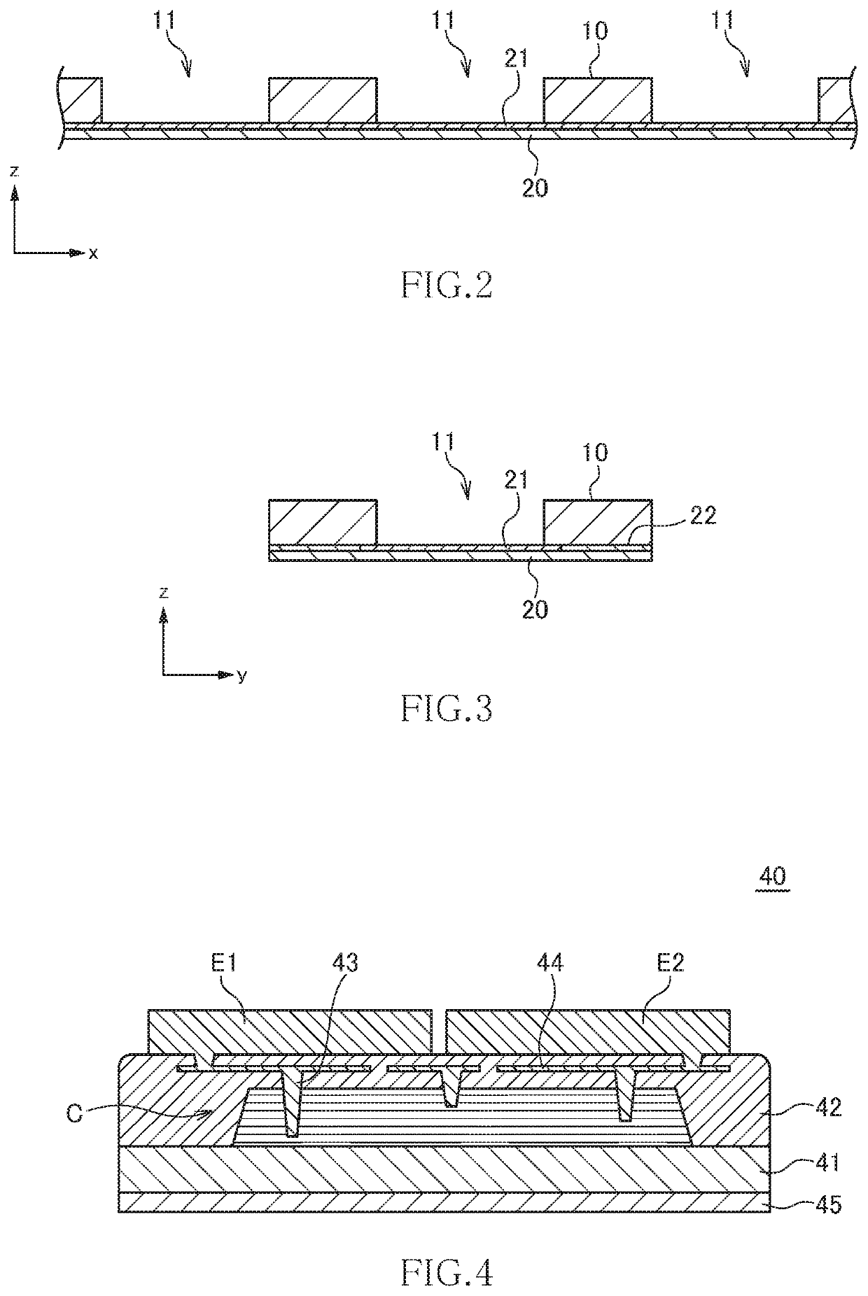
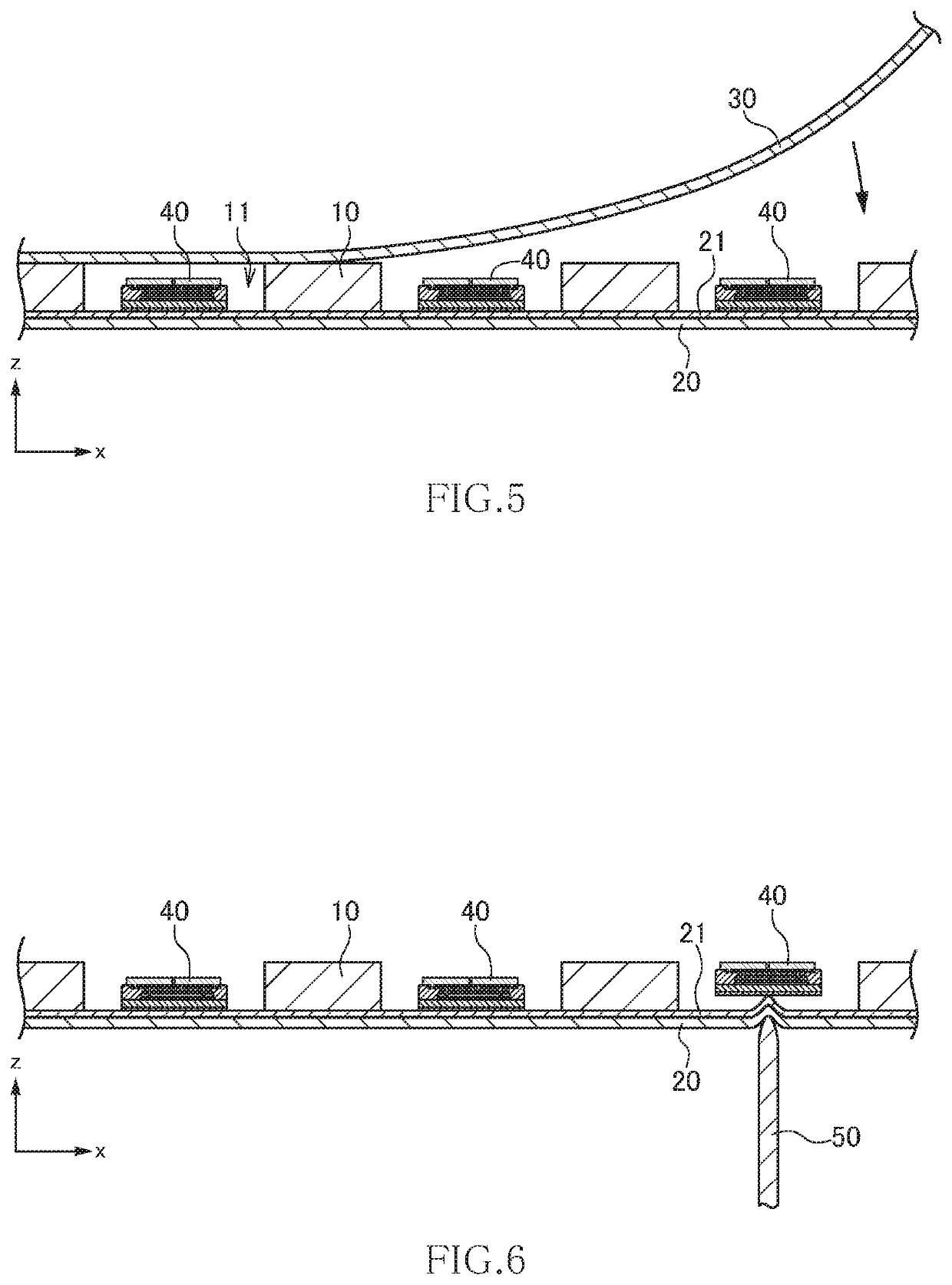
[0037]As illustrated in FIG. 1, an electronic component housing package 1 according to the present embodiment includes a carrier tape 10, a base film 20 stuck to one xy surface of the carrier tape 10, and a protective film 30 stuck to the other xy surface of the carrier tape 10. FIGS. 2 and 3 illustrate an A-A cross section and a B-B cross section of FIG. 1. In FIGS. 2 and 3, the protective film 30 is omitted for simplicity.

[0038]The carrier tape 10 is a support elongated in the x-direction and has a plurality of through holes 11 arranged in the x-direction so as to be spaced apart from one another at every certain interval. The through hole 11 provides a space for housing an electronic component and is formed penetrating the carrier tape 10 in the z-direction which is the thickness direction th...

second embodiment

[0050]FIG. 7 is a schematic exploded perspective view for explaining the configuration of an electronic component housing package 2 according to the second embodiment of the present invention.

[0051]As illustrated in FIG. 7, in the electronic component housing package 2 according to the present embodiment, the release layer 21 is not formed continuously, but a plurality of release layers 21 are formed intermittently in the x-direction each at a portion overlapping the though hole 11 with a slight margin therearound. In this point, the electronic component housing package 2 according to the present embodiment differs from the electronic component housing package 1 according to the first embodiment, and other configurations are the same as those of the electronic component housing package 1 according to the first embodiment, so the same reference numerals are given to the same elements, and overlapping description will be omitted.

[0052]As exemplified in the present embodiment, the rele...

third embodiment

[0053]FIG. 8 is a schematic exploded perspective view for explaining the configuration of an electronic component housing package 3 according to the third embodiment of the present invention.

[0054]As illustrated in FIG. 8, the electronic component housing package 3 according to the third embodiment differs from the electronic component housing package 2 according to the second embodiment in that the release layer 21 is formed only at the center of a portion overlapping the through hole 11. Other configurations are the same as those of the electronic component housing package 2 according to the second embodiment, so the same reference numerals are given to the same elements, and overlapping description will be omitted.

[0055]As exemplified in the present embodiment, a portion overlapping the through hole 11 may not be completely covered with the release layer 21, and it is sufficient that the release layer 21 is provided at a portion contacting at least the electronic component 40 or ...


PUM

PropertyMeasurementUnit
thicknessaaaaaaaaaa
degree of rigidityaaaaaaaaaa
areaaaaaaaaaaa

Abstract

Disclosed herein is an electronic component housing package that includes a carrier tape having a through hole for housing an electronic component, a base film stuck to the carrier tape and having a lower degree of rigidity than the carrier tape, and a release layer formed on a predetermined area of the base film so as to be exposed to the through hole of the carrier tape.

Description

BACKGROUND OF THE INVENTIONField of the Invention[0001]The present invention relates to an electronic component housing package and, more particularly, to a package for housing an electronic component stuck with an adhesive film such as a die attach film. The present invention also relates to a method of housing such an electronic component in an electronic component housing package.Description of Related Art[0002]As described in JP 1998-329866 A and JP 2012-236610 A, an electronic component housing package used in shipping electronic components is generally constituted by a carrier tape in which embossed recesses each housing an electronic component are formed.[0003]In recent years, demands for reduction in thickness of an electronic component such as a thin-film capacitor component or an IC chip have been increasing, and there exists an electronic component having a thickness smaller than 50 μm. Such an ultra-thin type electronic component is not easy to handle at mounting, so tha...

Claims


Application Information

Patent Timeline
Patent Type & Authority Applications(United States)
IPC IPC(8): H05K13/02B65D73/02H05K13/04H05K13/00B32B7/12C09J7/20
CPCB32B7/12H05K13/02B65D73/02H05K13/0084C09J7/20H05K13/0419B32B3/08B32B3/266B32B7/06B32B27/08B32B27/302B32B27/36B32B27/365B32B2255/10B32B2255/26B32B2307/202B32B2307/732B32B2307/748B32B2571/00B32B7/022
Inventor TOMIKAWA, MITSUHIROSATO, HIRONORI
Learn More