Multilayer ceramic electronic component

Active Publication Date: 2020-01-02
MURATA MFG CO LTD
View PDF0 Cites 6 Cited by
  • Summary
  • Abstract
  • Description
  • Claims
  • Application Information

AI Technical Summary

Benefits of technology

[0008]Preferred embodiments of the present invention provide small surface-mountable multilayer ceramic

Problems solved by technology

Although the film capacitors disclosed in Japanese Unexamined Patent Application Publications No. 2008-172050 and Japanese Unexamined Patent Application Publication No. 2008-277505 have sufficient creeping distances, the size thereof cannot be reduced due to structural reasons.
In addition, the film capacitors require lead terminals due to structural reasons, and may only be mounted by inserting the lead terminals into a mounting board.
Therefore, the film capacitors d

Method used


Image

  • Multilayer ceramic electronic component
  • Multilayer ceramic electronic component
  • Multilayer ceramic electronic component

Examples


first preferred embodiment

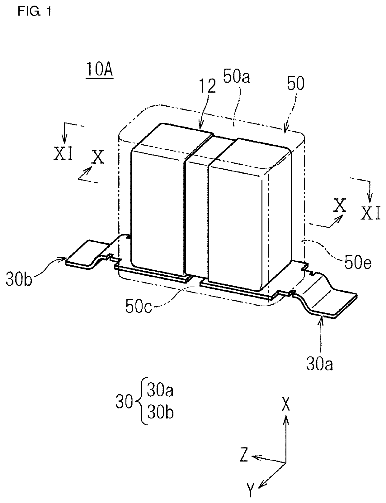
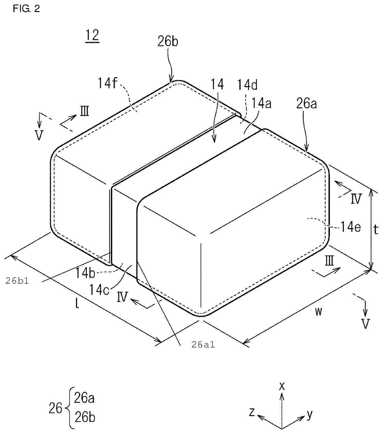
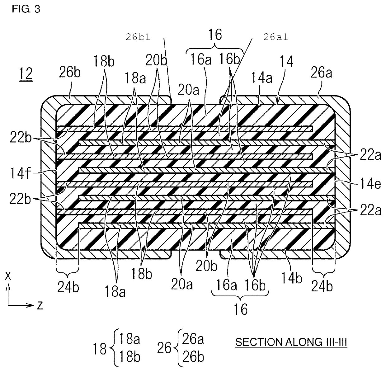
[0041]A multilayer ceramic electronic component according to a first preferred embodiment of the present invention will now be described. FIG. 1 is an external perspective view of an example of a multilayer ceramic electronic component according to a first preferred embodiment of the present invention. FIG. 2 is a perspective view illustrating the external shape of a multilayer ceramic electronic component body included in the multilayer ceramic electronic component illustrated in FIG. 1. FIG. 3 is a sectional view of the multilayer ceramic electronic component body illustrated in FIG. 2 taken along line III-III. FIG. 4 is a sectional view of the multilayer ceramic electronic component body illustrated in FIG. 2 taken along line IV-IV. FIG. 5 is a sectional view of the multilayer ceramic electronic component body illustrated in FIG. 2 taken along line V-V. FIG. 6 is a front view of the multilayer ceramic electronic component illustrated in FIG. 1. FIG. 7 is a side view of the multil...

second preferred embodiment

[0157]A multilayer ceramic electronic component according to a second preferred embodiment of the present invention will now be described. FIG. 13 is an external perspective view of an example of a multilayer ceramic electronic component according to a second preferred embodiment of the present invention. FIG. 14 is a front view of the multilayer ceramic electronic component illustrated in FIG. 13. FIG. 15 is a side view of the multilayer ceramic electronic component illustrated in FIG. 13. FIG. 16 is a top view of the multilayer ceramic electronic component illustrated in FIG. 13. FIG. 17 is a bottom view of the multilayer ceramic electronic component illustrated in FIG. 13. FIG. 18 is a sectional view of the multilayer ceramic electronic component illustrated in FIG. 13 taken along line XVIII-XVIII. FIG. 19 is a sectional view of the multilayer ceramic electronic component illustrated in FIG. 13 taken along line XIX-XIX. FIG. 20 is an external perspective view of metal terminals i...

third preferred embodiment

[0188]A multilayer ceramic electronic component according to a third preferred embodiment of the present invention will now be described. FIG. 21 is an external perspective view of an example of a multilayer ceramic electronic component according to a third preferred embodiment of the present invention. FIG. 22 is a front view of the multilayer ceramic electronic component illustrated in FIG. 21. FIG. 23 is a side view of the multilayer ceramic electronic component illustrated in FIG. 21. FIG. 24 is a top view of the multilayer ceramic electronic component illustrated in FIG. 21. FIG. 25 is a bottom view of the multilayer ceramic electronic component illustrated in FIG. 21. FIG. 26 is a sectional view of the multilayer ceramic electronic component illustrated in FIG. 21 taken along line XXVI-XXVI. FIG. 27 is a sectional view of the multilayer ceramic electronic component illustrated in FIG. 21 taken along line XXVII-XXVII. FIG. 28 is an external perspective view of metal terminals i...


PUM

PropertyMeasurementUnit
Fractionaaaaaaaaaa
Fractionaaaaaaaaaa
Thicknessaaaaaaaaaa

Abstract

A multilayer ceramic electronic component includes a multilayer ceramic electronic component body and a pair of metal terminals. The multilayer ceramic electronic component body includes a multilayer body including laminated ceramic layers and inner electrode layers and first and second outer electrodes provided on both end surfaces of the multilayer body. The metal terminals are connected to the outer electrodes. The inner electrode layers are perpendicular or substantially perpendicular to a mounting surface and include extended portions that extend to the end surfaces and portions of the first and second side surfaces. The distance between ends of the first and second outer electrodes on one of the first and second side surfaces is in a range from about 1.8% to about 31.3% of a length dimension of the multilayer ceramic electronic component in a direction connecting both end surfaces of the multilayer ceramic electronic component body.

Description

CROSS REFERENCE TO RELATED APPLICATIONS[0001]This application claims the benefit of priority to Japanese Patent Application No. 2018-122473 filed on Jun. 27, 2018. The entire contents of this application are hereby incorporated herein by reference.BACKGROUND OF THE INVENTION1. Field of the Invention[0002]The present invention relates to multilayer ceramic electronic components including metal terminals, and more particularly, to multilayer ceramic electronic components each including two metal terminals connected to outer electrodes of multilayer ceramic electronic component bodies.2. Description of the Related Art[0003]In recent years, inverter circuits suitable for achieving less energy consumption and higher efficiency have been used in consideration of environmental protection. With increasing working voltage, electronic components operable at higher voltages and currents have been desired.[0004]When an electronic component, such as a multilayer ceramic capacitor, is operated at...

Claims


Application Information

Patent Timeline
IPC IPC(8): H01G4/248H01G4/30H01G4/012H01G4/232H01G4/38H01G4/224H01G4/12
CPCH01G4/38H01G4/1227H01G4/2325H01G4/248H01G4/012H01G4/30H01G4/1236H01G4/224H01G4/232H01G4/228H01G4/12H01G2/065H01G2/14
Inventor ITAMOCHI, MASAKAZU
Owner MURATA MFG CO LTD
Why Eureka
Try Eureka