Glue filling method for multilayer thin film sensor structure

a multi-layer thin film and sensor technology, applied in the direction of instruments, other domestic objects, force measurement, etc., can solve the problems of difficult to meet demand, traditional manufacturing process is likely to fail in filling conductive, and the fabrication process is more complicated. , to achieve the effect of fine interface compatibility and facilitate the formation of arc-shaped bumps

Active Publication Date: 2020-01-09
INTERFACE TECH CHENGDU CO LTD +2
View PDF5 Cites 0 Cited by
  • Summary
  • Abstract
  • Description
  • Claims
  • Application Information

AI Technical Summary

Benefits of technology

[0006]The primary objective of the present invention is to provide a glue filling method for a multilayer thin film sensor structure, which uses a multilayer composite heat-resistant membrane to facilitate forming an arc-shaped bump on the bottom of the conductive glue in the glue filling process, whereby the conductive glue can cover a portion of the lower conductive metal layer to enable the electric connection of the multilayer thin film sensor structure, and whereby are achieved a water-proof effect and an airtight effect, and whereby is acquired a fine interface compatibility.

Problems solved by technology

The more sophisticated the functions of touchscreens grow, the more complicated the fabrication process thereof would be.
The existing technology has been hard to meet demand.
The traditional manufacture process is likely to fail in filling conductive glue for the current multilayer thin film sensor structures.
However, the conventional technology fails to form a lower conductive bump on the bottom of the conductive glue 1.
Besides, while the conductive glue 1 is filled into the electric-conduction through-holes, the conventional technology may suffer incomplete glue filling or fail to electrically connect the conductive metal layers, which would disable the signal communication between the upper and lower layers of the thin film sensor structure 2.

Method used


Image

  • Glue filling method for multilayer thin film sensor structure
  • Glue filling method for multilayer thin film sensor structure
  • Glue filling method for multilayer thin film sensor structure

Examples


Embodiment Construction

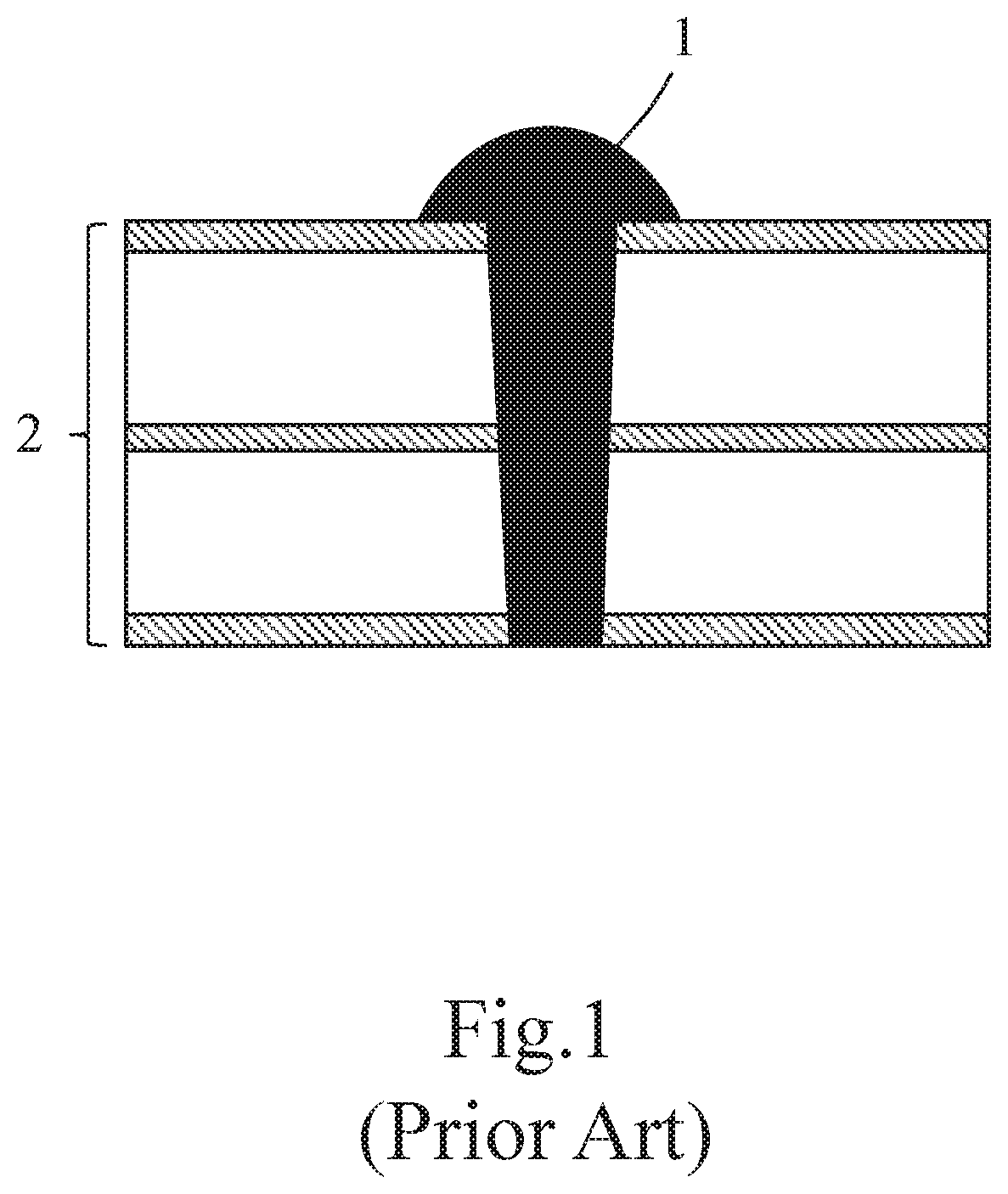
[0025]The present invention discloses a glue filling method for a multilayer thin film sensor structure, which is applicable to multilayer thin film sensor structures and characterized in using a composite heat-resistant membrane to function as a sustaining layer in filling a conductive glue, whereby the conductive glue is fully filled into the electric-conduction through-hole and formed to be a convex cover having a special shape for covering the conductive metal on the bottom of the multilayer thin film sensor structure.

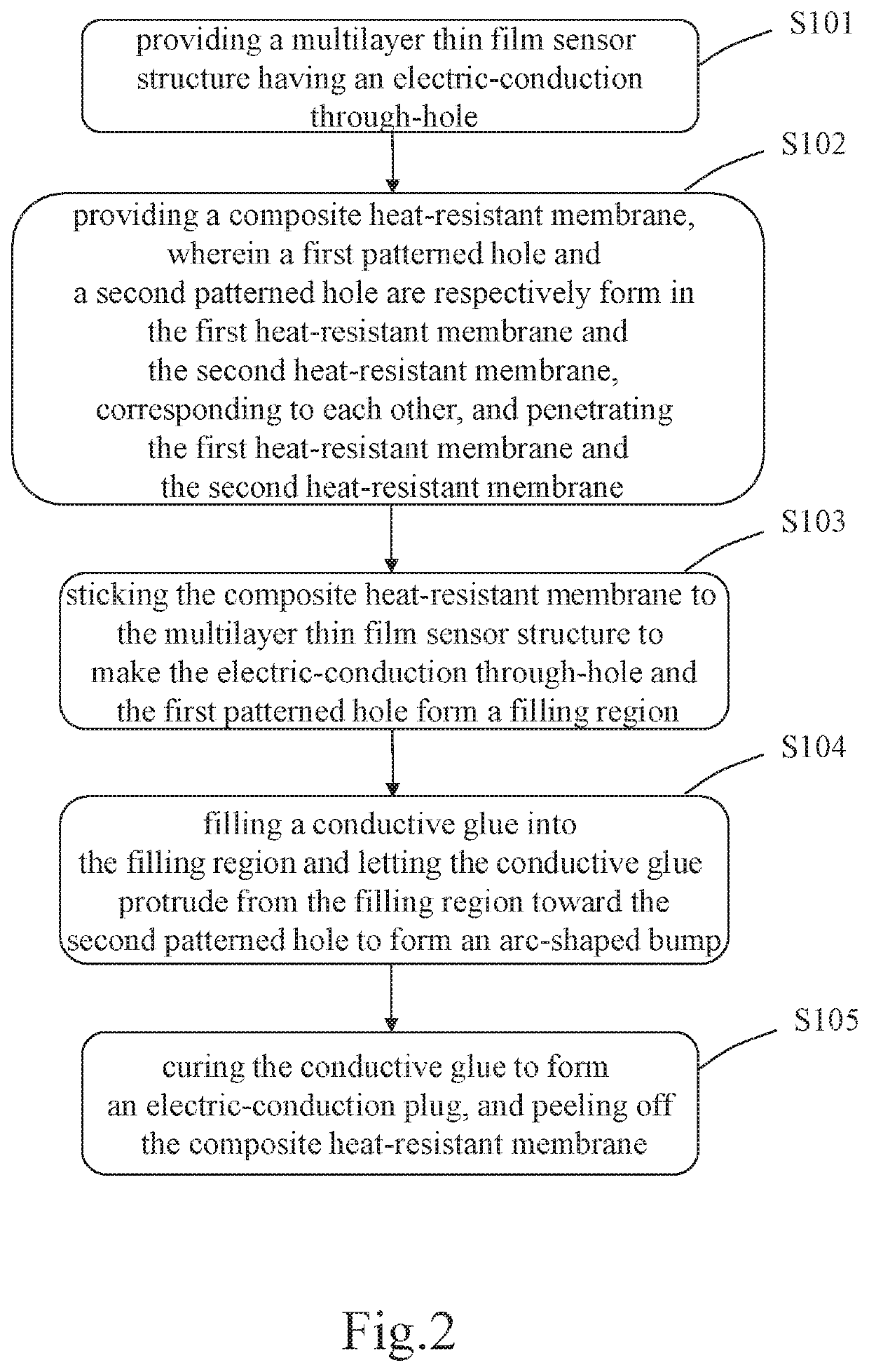
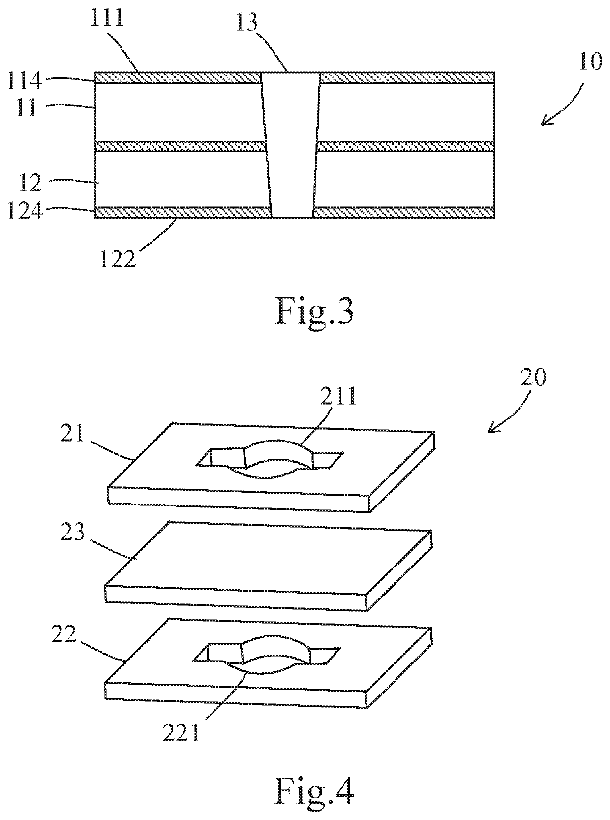
[0026]Refer to FIG. 2 for a flowchart of a glue filling method for a multilayer thin film sensor structure according to one embodiment of the present invention. Also refer to FIGS. 3-7, which are diagrams schematically showing the steps of a glue filling method for a multilayer thin film sensor structure according to one embodiment of the present invention. The method of the present invention comprises Steps S101-S105.

[0027]In Step S101, provide a multilayer thin f...


PUM

PropertyMeasurementUnit
electric-conductionaaaaaaaaaa
heat-resistantaaaaaaaaaa
sizesaaaaaaaaaa

Abstract

A glue filling method for a multilayer thin film sensor structure is disclosed herein. Two outer layers of a composite heat-resistant membrane are carved to have desired patterned holes; an inner layer is interposed between two outer layers to form a layered structure. The composite heat-resistant membrane is stuck onto the multilayer thin film sensor structure with the patterned holes aligned to an electric-conduction through-hole of the multilayer thin film sensor structure to form a filling region. A conductive glue is filled into the filling region. Sustained by the inner-layer heat-resistant membrane, the conductive glue protrudes from the patterned hole to cover a portion of the conductive metals on the surface of the multilayer thin film sensor structure. Thereby are simultaneously achieved a water-proof effect, an airtight effect and a fine interface compatibility.

Description

[0001]This application claims priority for China patent application no. 201810744459.0 filed on Jul. 9, 2018, the content of which is incorporated by reference in its entirety.BACKGROUND OF THE INVENTIONField of the Invention[0002]The present invention relates to a multilayer thin film sensor structure, particularly to a glue filling method for a multilayer thin film sensor structure, which can guarantee electric conductivity.Description of the Related Art[0003]Owing to advance of science and technology, portable electronic devices, such as notebook computers, tablet computers, smart phones, etc., have been very popular in daily life, and the functions thereof are being enhanced persistently. The portable electronic devices normally have a touchscreen, which not only displays audio and video multimedia information to users but also provides a convenient operating interface for users. Recently, manufacturers have tended to equip portable electronic devices with a larger touchscreen t...

Claims


Application Information

Patent Timeline
Patent Type & Authority Applications(United States)
IPC IPC(8): C09J9/02G01L1/20C09J5/00
CPCC09J5/00C09J9/02G01L1/205B32B37/1284G06F3/0412B32B3/266B32B9/041B32B15/04B32B2250/05B32B2250/42B32B2307/202B32B2307/306B32B2307/412B32B2307/7265B32B2457/00B29C65/70B29C65/741B29C65/76B29C65/7808B29C65/7844B29C66/02242B29C66/304B29C66/41B29C66/723B29C66/72321B29C66/73141B32B38/10B32B43/006Y10T156/11Y10T156/1168Y10T156/19
Inventor CHEN, SHENG CHEHO, YI-HUNG
Owner INTERFACE TECH CHENGDU CO LTD
Why Eureka
Try Eureka