Display panel and method of manufacturing the same

a technology of display panel and display panel, which is applied in the field of display panel, can solve the problems of inability to appropriately solve the temporary problems of the relevant circuit, and the resistance-capacitance load of the relevant circuit is too large, so as to reduce the resistance-capacitance load of the circuit, the effect of slowing down

Inactive Publication Date: 2020-01-30
HKC CORP LTD +1
View PDF5 Cites 0 Cited by
  • Summary
  • Abstract
  • Description
  • Claims
  • Application Information

AI Technical Summary

Benefits of technology

[0009]In view of the above-mentioned drawbacks of the prior art, the primary object of the present disclosure is to provide a display panel and a method for manufacturing the same capable of slowing down and reducing the resistance-capacitance load of the circuit.

Problems solved by technology

But GOA technology has some temporary problems cannot be appropriately solved, for example, the resistance-capacitance load of the relevant circuit is too large.

Method used


Image

  • Display panel and method of manufacturing the same
  • Display panel and method of manufacturing the same
  • Display panel and method of manufacturing the same

Examples


Embodiment Construction

[0023]In order to make a better understanding of the technical solutions in the present application to those skilled in the art, the technical solutions in the embodiments of the present application will be described clearly and completely with reference to the drawings in the embodiments of the present application. Apparently, the embodiments described are merely partial embodiments of the present application, rather than all embodiments. Other embodiments figured out by those skilled in the art on the basis of the embodiments of the invention without going through creative efforts shall all fall within the protection scope of the present application.

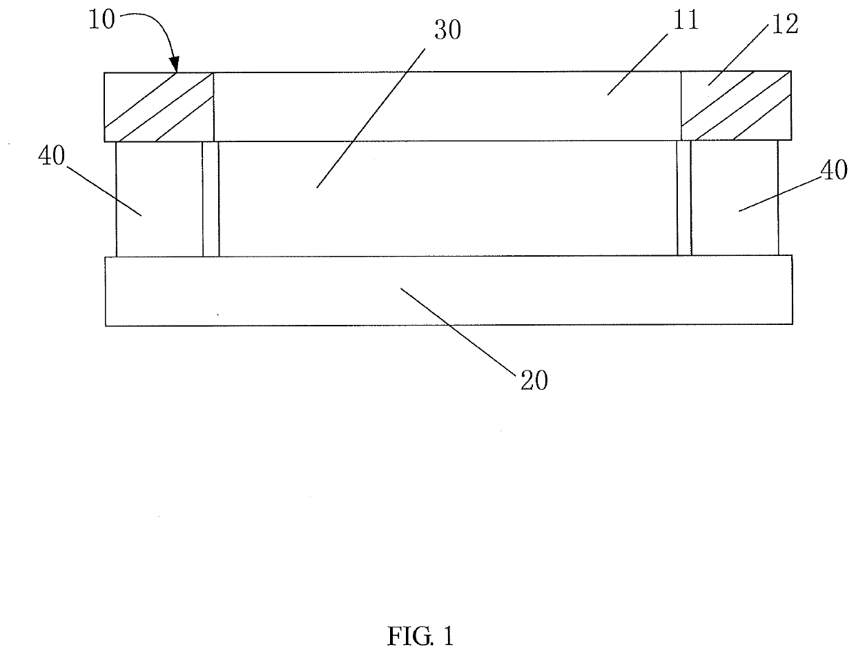
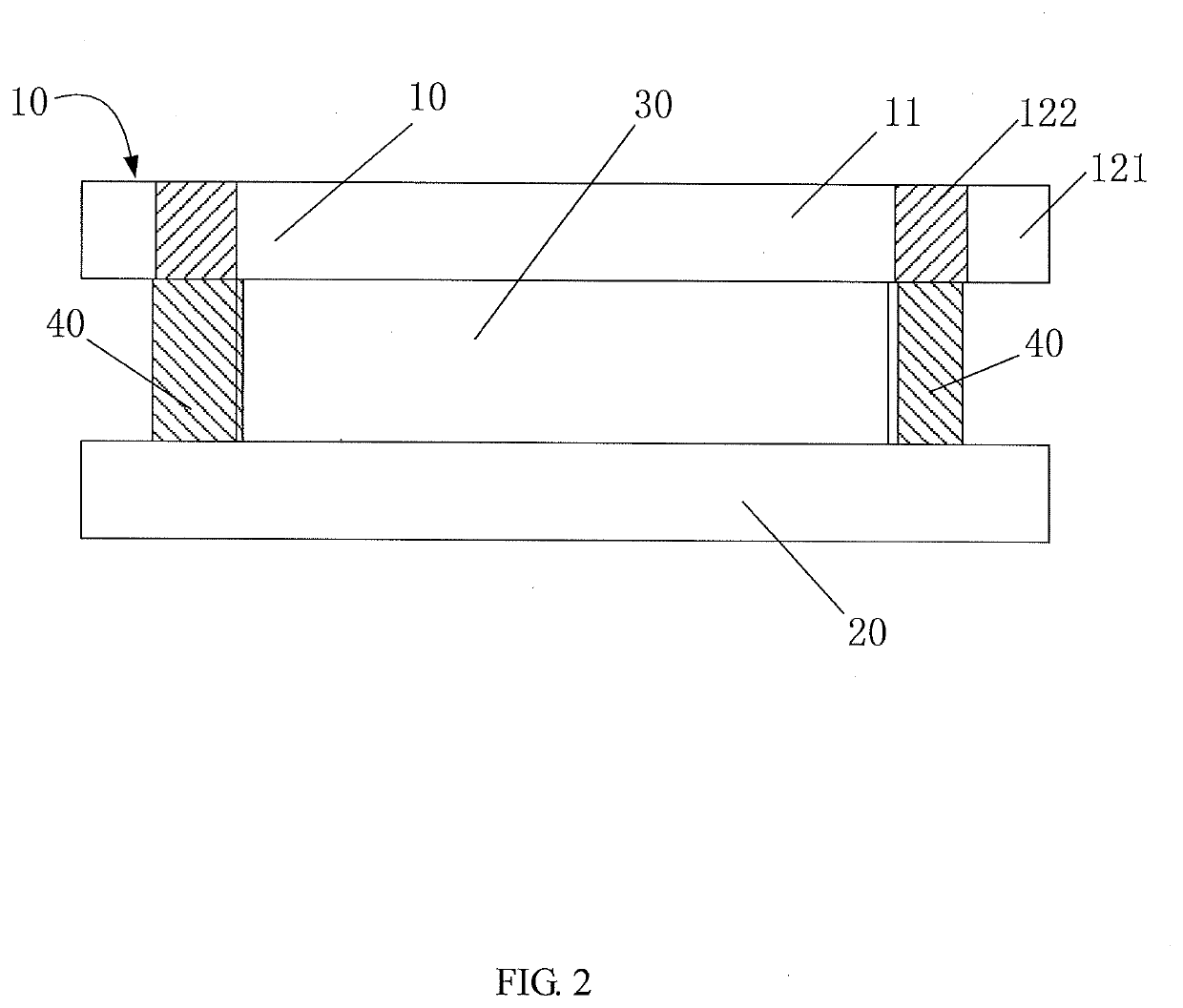
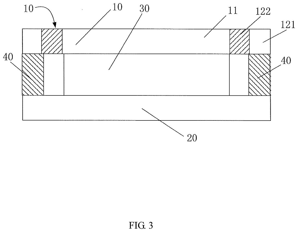
[0024]FIG. 1 is a schematic view of a display panel of the present invention for reducing the resistance-capacitance load of a circuit, the display panel includes:

[0025]A first substrate 10;

[0026]A second substrate 20 includes a color filter layer (not shown in figure) and be disposed opposite to the first substrate 10;

[0027]A liquid c...


PUM

PropertyMeasurementUnit
dielectric constantaaaaaaaaaa
areaaaaaaaaaaa

Abstract

A display panel and a method for manufacturing the same are provided. The display panel includes a first substrate, a second substrate including a color filter layer and disposed opposite to the first substrate, and a liquid crystal layer disposed between the first substrate and the second substrate. The first substrate includes a circuit area and a display area. The circuit area is formed with a spacer layer, a dielectric constant of the spacer layer is lower than a dielectric constant of the liquid crystal layer.

Description

CROSS-REFERENCE TO RELATED APPLICATION[0001]This application claims the benefit of China Patent Application No. 201710546034.4, filed on Jul. 6, 2017, in the State Intellectual Property Office of the People's Republic of China, the disclosure of which is incorporated herein in its entirety by reference.FIELD OF THE INVENTION[0002]The present invention relates to the display technology, and more particularly to a display panel for reducing the resistance-capacitance load of a circuit and a method for manufacturing the same.BACKGROUND OF THE INVENTION[0003]With the development and progress of science and technology, a liquid crystal display has the advantages of a thin body, energy-saving, no radiation and so on, and thus becomes the mainstream of the display products and widely used. Most of the liquid crystal displays on the market are of the backlight-type, which includes a liquid crystal panel and a backlight module. The liquid crystal panel includes two parallel glass substrates ...

Claims


Application Information

Patent Timeline
Patent Type & Authority Applications(United States)
IPC IPC(8): G02F1/1339G02F1/1345G02F1/1362
CPCG02F1/13452G02F2001/13398G02F1/13394G02F1/13454G02F1/136286G02F2202/022G02F1/13306G09G3/36G02F1/13398G02F1/13606
Inventor CHEN, YU-JEN
Owner HKC CORP LTD
Why Eureka
Try Eureka