Method of making a plurality of printed circuit boards from a single circuit board sheet

a technology of printed circuit boards and single circuit boards, which is applied in the direction of sustainable manufacturing/processing, coupling device connection, final product manufacturing, etc., can solve the problems of wasting resources, adding the task of cutting to the process, and the disconnector cannot be disposed near the other sid

Active Publication Date: 2020-02-13
CANON KK
View PDF0 Cites 0 Cited by
  • Summary
  • Abstract
  • Description
  • Claims
  • Application Information

AI Technical Summary

Benefits of technology

This patent describes a method for making multiple printed circuit boards with the same connector layout. The method involves creating a single circuit board sheet and then mounting connectors on one side of the sheet while melting solder paste onto the opposite side. The sheet is then separated along a line, and new connectors are mounted on the other side. This process allows for the creation of identical circuit boards with simplified assembly.

Problems solved by technology

Although surface-mounted connectors can be mounted on both the front and rear surfaces of a printed circuit board, such connectors cannot be disposed near the other side.
The holding region is cut away and discarded as a throwaway board, which wastes resources and adds the task of cutting to the process.
When a worker bends the circuit board sheet in order to cut the sheet, the plurality of connectors disposed on both sides of the separation line interfere (collide) with each other.
The interference between the plurality of connectors makes it impossible to bend the circuit board sheet to an angle at which the sheet can be cut.

Method used


Image

  • Method of making a plurality of printed circuit boards from a single  circuit board sheet
  • Method of making a plurality of printed circuit boards from a single  circuit board sheet
  • Method of making a plurality of printed circuit boards from a single  circuit board sheet

Examples


first embodiment

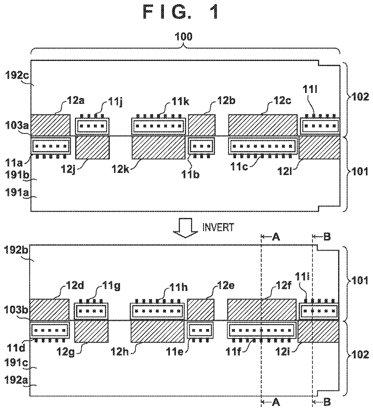
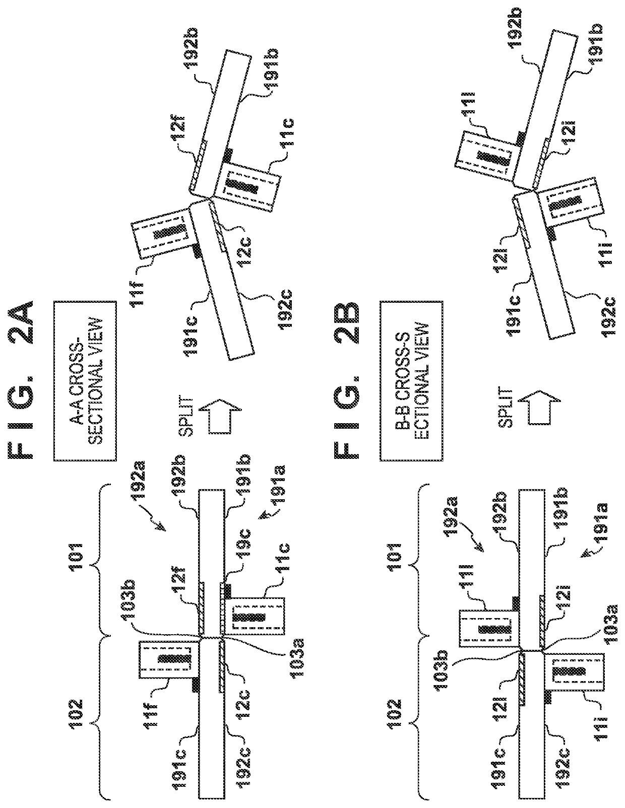
[0019]FIG. 1 is a diagram illustrating reversible imposition. Note that the reference signs are constituted by numbers and letters. When several reference signs having the same number refer to common items, the letters are dropped from the reference signs. A circuit board sheet 100 has a first printed circuit board 101 and a second printed circuit board 102. Separation lines 103a and 103b are provided between the first printed circuit board 101 and the second printed circuit board 102. The separation lines 103a and 103b are joints (perforations) or grooves (V-cuts) for making it easy to separate (split or cut) the first printed circuit board 101 and the second printed circuit board 102, for example. The circuit board sheet 100 has a front surface 191a and a rear surface 192a. The separation line 103a is provided on the front surface 191a of the circuit board sheet 100. The separation line 103b is provided on the rear surface 192a of the circuit board sheet 100. The first printed cir...

second embodiment

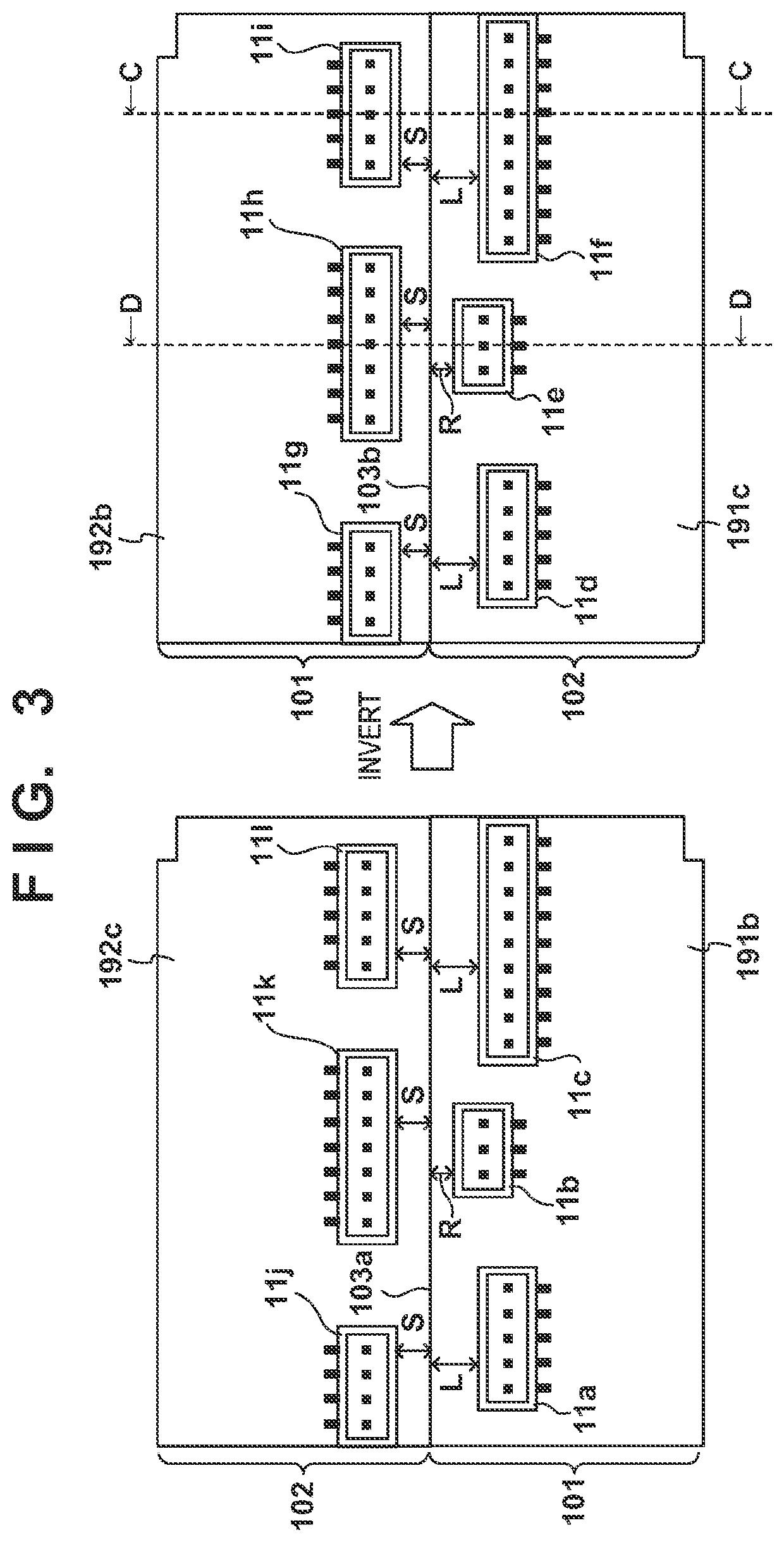
[0029]In the first embodiment, of two regions on the circuit board sheet 100 adjacent to each other with the separation line 103 therebetween, one of the regions serves as a connector mounting region, and the other serves as a non-mounting region. This suppresses interference between connectors and makes it possible to bend the circuit board sheet 100 and separate the sheet into a plurality of printed circuit boards. The second embodiment introduces a solution that is different from that described in the first embodiment. There are cases where both regions on the circuit board sheet 100 adjacent to each other with the separation line 103 therebetween serve as connector mounting regions. Connector layout conditions which ensure that even if the circuit board sheet 100 is bent in such a case, the connectors mounted in the one region will not interfere with the connectors mounted in the other region, will be described here. The “connector layout conditions” are defined by, for example,...

third embodiment

[0038]In the second embodiment, the cable insertion direction of the connectors 11g to 11l is what is called the vertical direction. Such connectors may be called a “vertical type”. In the third embodiment, the cable insertion direction of the connectors 11g to 11l is changed what is called the horizontal direction. Note that “horizontal” means being parallel to the front surface 191a and the rear surface 192a of the circuit board sheet 100. Such connectors may be called a “horizontal type”. Note that the “vertical direction” is the direction parallel to the normal direction of the first printed circuit board 101 and the second printed circuit board 102. The “horizontal direction” is the direction orthogonal to the normal direction of the first printed circuit board 101 and the second printed circuit board 102.

[0039]With the first printed circuit board 101 and the second printed circuit board 102 described in the first and second embodiments, vertical type connectors 11a to 11l are ...


PUM


Abstract

A solder paste is printed on a first surface of a sheet. Connectors are mounted on a first surface of a first board and a second surface of a second board. The sheet is inverted. A solder paste is printed on a second surface of the sheet. Connectors are mounted on a second surface of the first board and a first surface of the second board. The solder paste printed onto the second surface of the sheet is melted. The first board is separated from the second board. The first and second board have the same connector layout. A first connector soldered to the first surface of the first board and a second connector soldered to the second surface of the second board are disposed at a location where the sheet can be bent and broken along the separation line.

Description

BACKGROUND OF THE INVENTIONField of the Invention[0001]The present invention relates to a method of making a plurality of printed circuit boards from a single circuit board sheet.Description of the Related Art[0002]Various types of connectors are arranged on printed circuit boards. Japanese Patent Laid-Open No. 2005-26246 discloses mounting surface-mounted connectors on a printed circuit board. Such connectors are soldered to the surface of the printed circuit board in a reflow oven. Using surface-mounted connectors eliminates the need for through-holes for inserting the terminals of the connectors into the printed circuit board. Japanese Patent Laid-Open No. 2005-44855 discloses reversible imposition. Generally speaking, a method of mass-producing multiple printed circuit boards having the same circuit configuration by dividing a single circuit board sheet is called “imposition”. “Reversible imposition” is imposition in which the layout pattern of electronic components mounted on t...

Claims


Application Information

Patent Timeline
IPC IPC(8): H01R43/02H01R12/71H01R12/51H01R12/75H05K3/34H05K3/00H05K1/18
CPCH01R43/0256H01R12/75H05K2201/1031H05K3/0097H05K3/3415H05K2203/302H01R12/716H01R12/51H05K1/181H05K2201/10356H05K2201/10545H05K2201/10189H05K3/0052H05K2203/1476H05K2203/1572Y02P70/50
Inventor SUGIYAMA, NORIKAZU
Owner CANON KK
Why Eureka
Try Eureka