Wafer-level assembly method for chip-size devices having flipped chips

a chip-size, leadless technology, applied in semiconductor devices, semiconductor/solid-state device details, electrical equipment, etc., can solve the problems of large capital cost, unfriendly environment, and high cost of wire bonding assembly, so as to improve the reliability of the device, reduce manufacturing cost, and improve the thermal performance of the package

Inactive Publication Date: 2005-07-14
TEXAS INSTR INC
View PDF8 Cites 50 Cited by
  • Summary
  • Abstract
  • Description
  • Claims
  • Application Information

AI Technical Summary

Benefits of technology

[0013] It is a technical advantage of the present invention that a wide variety of materials and techniques can be employed for the proposed metallization and assembly steps.
[0014] Other technical advantages of the present invention include a reduction of manufacturing cost, a lead-free assembly solution, improved thermal performance of the package

Problems solved by technology

There are several issues with the bumped flip-chip approach.
First, the technology is expensive compared to conventional wire bonding assembly.
The typical solder bumping process is very equipment intensive, resulting in a large capital cost.
The application of pre-fabricated solder balls and the evaporation, plating, or screening of solder material are environmentally unfriendly in that they make use of excess of solder, often containing lead.
Both processing and clean-up costs are high in these operations.
Second, the manufacturing of flip-chip assembly can have a long cycle time.
These furnaces are usually very long (>3 m) and massive structures, occupying much space on the assembly floor.
Moving parts in such furnaces are a significant source of particulate contamination.
Third, several metallurgical solder fillet

Method used


Image

  • Wafer-level assembly method for chip-size devices having flipped chips
  • Wafer-level assembly method for chip-size devices having flipped chips
  • Wafer-level assembly method for chip-size devices having flipped chips

Examples


Embodiment Construction

[0025] The present invention is related to U.S. patent Applications No. 10 / 001,302, filed on Oct. 01, 2001 (Zuniga-Ortiz et al., “Bumpless Wafer Scale Device and Board Assembly”); No. 10 / 057,138, filed on Jan. 25, 2002 (Zuniga-Ortiz et al., “Flip-Chip without Bumps and Polymer for Board Assembly”); No. 10 / 678,709, filed on Oct. 3, 2003 (Bojkov et al., “Sealing and Protecting Integrated Circuit Bonding Pads”); and No. 10 / 689,386, filed on Oct. 20, 2003 (Bojkov et al., “Direct Bumping on Integrated Circuit Contacts Enabled by Metal-to-Insulator Adhesion”).

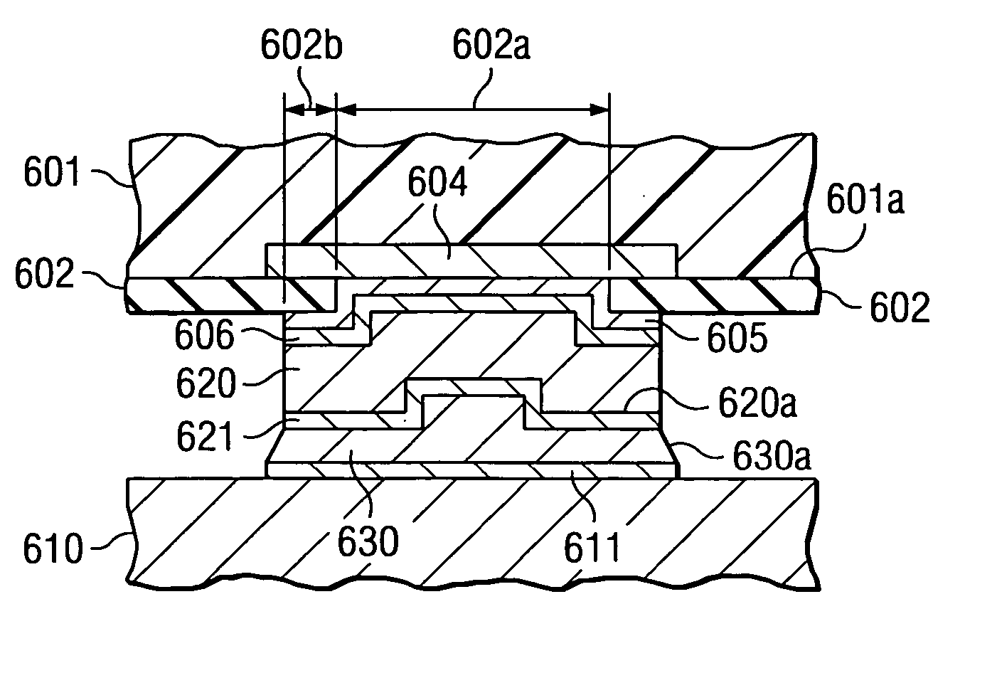
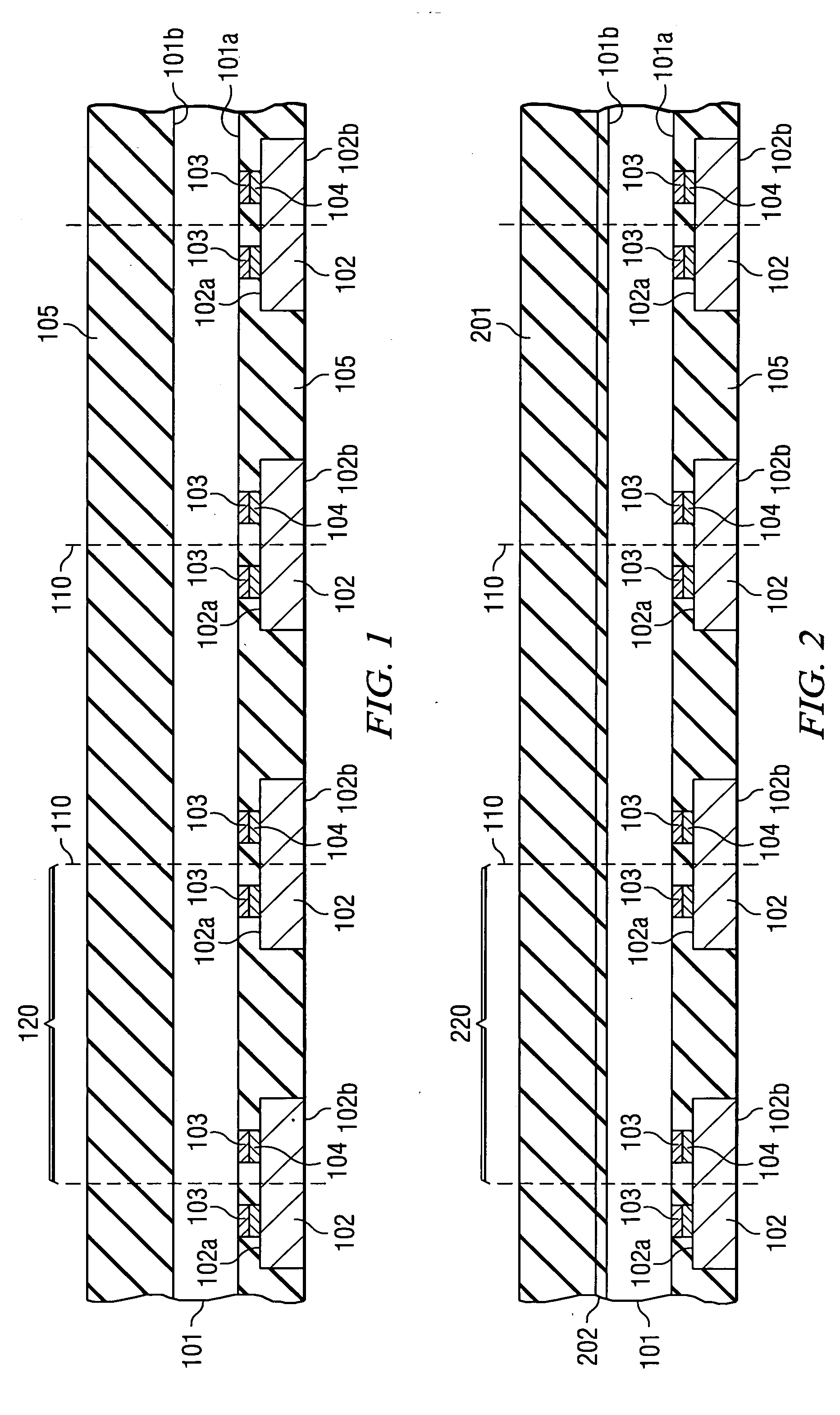
[0026] The schematic cross section of FIG. 1 shows an embodiment of the invention. A semiconductor wafer 101 with an active surface 101a is assembled on a leadframe, which has a plurality of leadframe segments 102. The assembly is performed by means of attaching the plurality of contact studs 103 (more detail below) of the active wafer surface with solder paste 104. An encapsulation material (preferably a molding compound) 105 cover...


PUM


Abstract

A method for assembling a whole semiconductor wafer (101) with a plurality of device units (120) having metal contact pads. Each contact pad has a patterned barrier metal layer and a metal stud (103, preferably copper or nickel) with an outer surface suitable to form metallurgical bonds without melting. A leadframe suitable for the whole wafer is provided, which has a plurality of segments groups (102), each group suitable for one device unit; each segment has first (102a) and second ends (102b) covered by solderable metal. A predetermined amount of solder paste (104) is placed on each of the first segment ends. The leadframe is then aligned with the wafer so that each of the paste-covered segment ends is aligned with the corresponding metal stud of the respective device unit. The leadframe is connected to the wafer and the whole wafer is encapsulated (105) so that the device units and the first segment ends are covered, while the second segment ends remain exposed. The encapsulated wafer is separated (110) into individual device units (120).

Description

FIELD OF THE INVENTION [0001] The present invention is related in general to the field of electronic systems and semiconductor devices and more specifically to a wafer-level assembly method for chip-size, leadless devices having chips flip-assembled without bumps. DESCRIPTION OF THE RELATED ART [0002] The fabrication of semiconductor devices is commonly based on assembly and packaging of individual semiconductor chips. One type of such assembly is the flip-chip technology, which uses either solder bumps (often referred to as solder balls) or gold bumps to attach the chip to a substrate, or to attach a package device to an external part. [0003] There are several issues with the bumped flip-chip approach. First, the technology is expensive compared to conventional wire bonding assembly. The typical solder bumping process is very equipment intensive, resulting in a large capital cost. The application of pre-fabricated solder balls and the evaporation, plating, or screening of solder ma...

Claims


Application Information

Patent Timeline
IPC IPC(8): H01L23/31H01L23/495
CPCH01L23/3114H01L2224/13099H01L24/13H01L24/16H01L24/94H01L2224/16245H01L2224/73253H01L24/81H01L2224/13082H01L2224/81193H01L2224/94H01L23/4951H01L2224/13019H01L2224/81H01L24/05H01L2224/0401H01L2224/05001H01L2224/05022H01L2224/05027H01L2224/05124H01L2224/05147H01L2224/05166H01L2224/05171H01L2224/05181H01L2224/05184H01L2224/05572H01L2224/05624H01L2224/05644H01L2224/05647H01L2224/05655H01L2224/05664H01L2224/05666H01L2224/05671H01L2224/05681H01L2224/05684H01L2924/12042H01L2924/14H01L2924/181H01L2924/00H01L2924/00014
Inventor BOYD, WILLIAM D.HAGA, CHRISCOYLE, ANTHONY L.SWANSON, LELAND S.MAI, QUANG X.
Owner TEXAS INSTR INC
Why Eureka
Try Eureka