On-chip test circuit for assessing chip integrity

a test circuit and chip integrity technology, applied in the direction of semiconductor devices, semiconductor/solid-state device details, instruments, etc., can solve the problems of circuit chip failure, low-k dielectric materials with relatively lower mechanical strength than conventional silicon oxide dielectrics such as fsg or usg, and some drawbacks of sam techniqu

Active Publication Date: 2007-02-01
UNITED MICROELECTRONICS CORP
View PDF3 Cites 50 Cited by
  • Summary
  • Abstract
  • Description
  • Claims
  • Application Information

AI Technical Summary

Problems solved by technology

However, one shortcoming associated with the use of low-k dielectrics is that almost all low-k dielectric materials possess relatively lower mechanical strength than that of conventional silicon oxide dielectrics such as FSG or USG.
The use of low-k dielectrics poses this industry another problem that the adhesion ability, either at the interface between two adjacent low-k dielectric layers or at the interface between a low-k dielectric layer and a dissimilar dielectric layer, is somewhat inadequate to meet the requirements in the subsequent wafer treatment processes such as wafer dicing, which is typically performed to mechanically cut a semiconductor wafer into a number of individual IC chips.
Delamination or cracking that occurs during scribing, dicing or temperature cycling test is problematic and may cause circuit chip failures.
However, the SAM technique has some drawbacks.
During the bare die check after dicing, very small cracks are difficult to detect because of the detection limit of the SAM tools.
On the other hand, even the delamination defect is detectable it is often difficult to characterize the specific location of the defect for the packaged IC check.
That is, the information whether the defect is in the interlayer of the IC chip or at the interface between the IC chip and packaging material is not available.

Method used


Image

  • On-chip test circuit for assessing chip integrity
  • On-chip test circuit for assessing chip integrity
  • On-chip test circuit for assessing chip integrity

Examples


Embodiment Construction

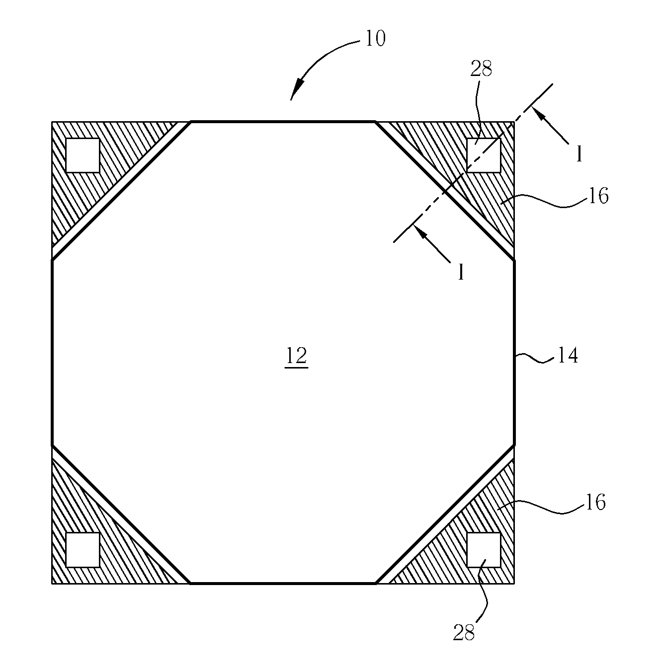
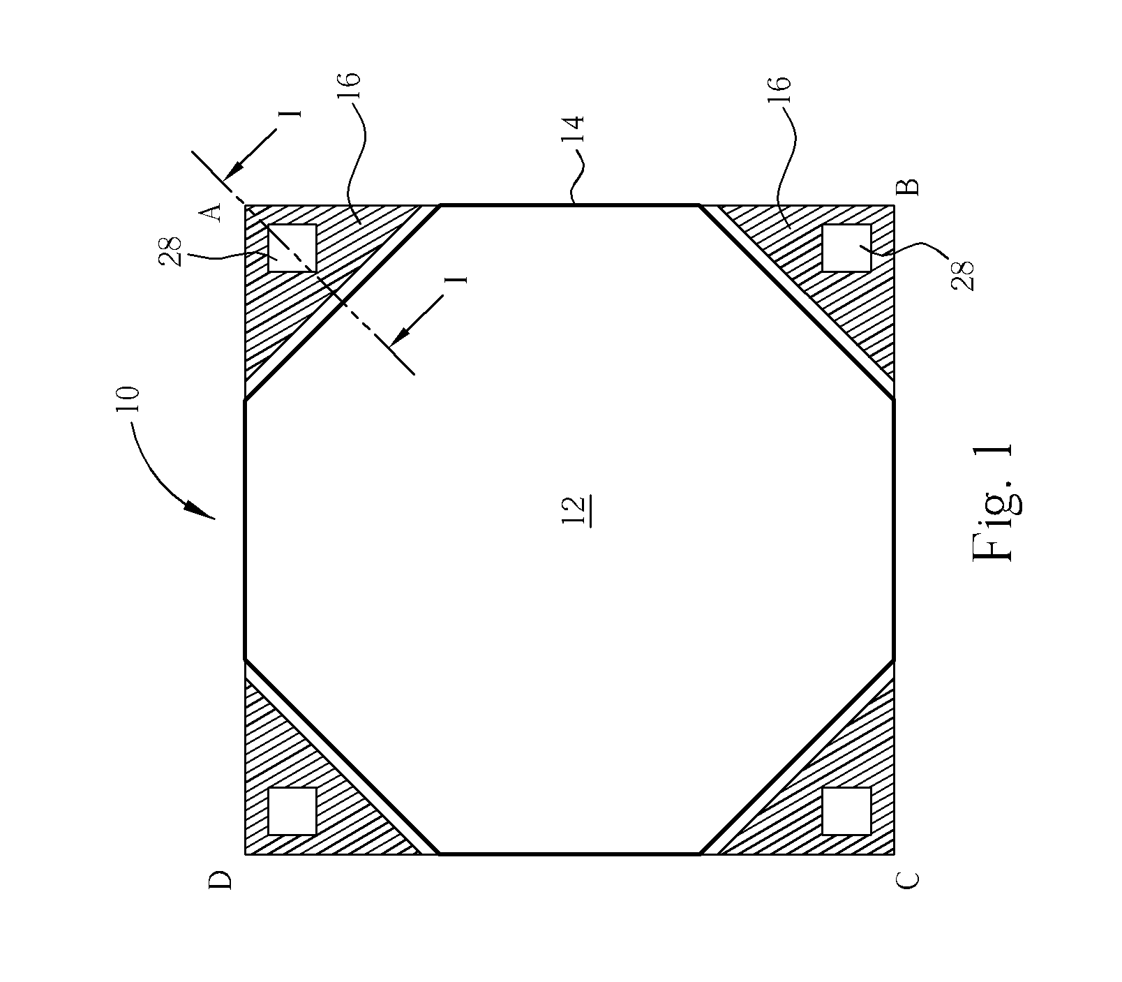
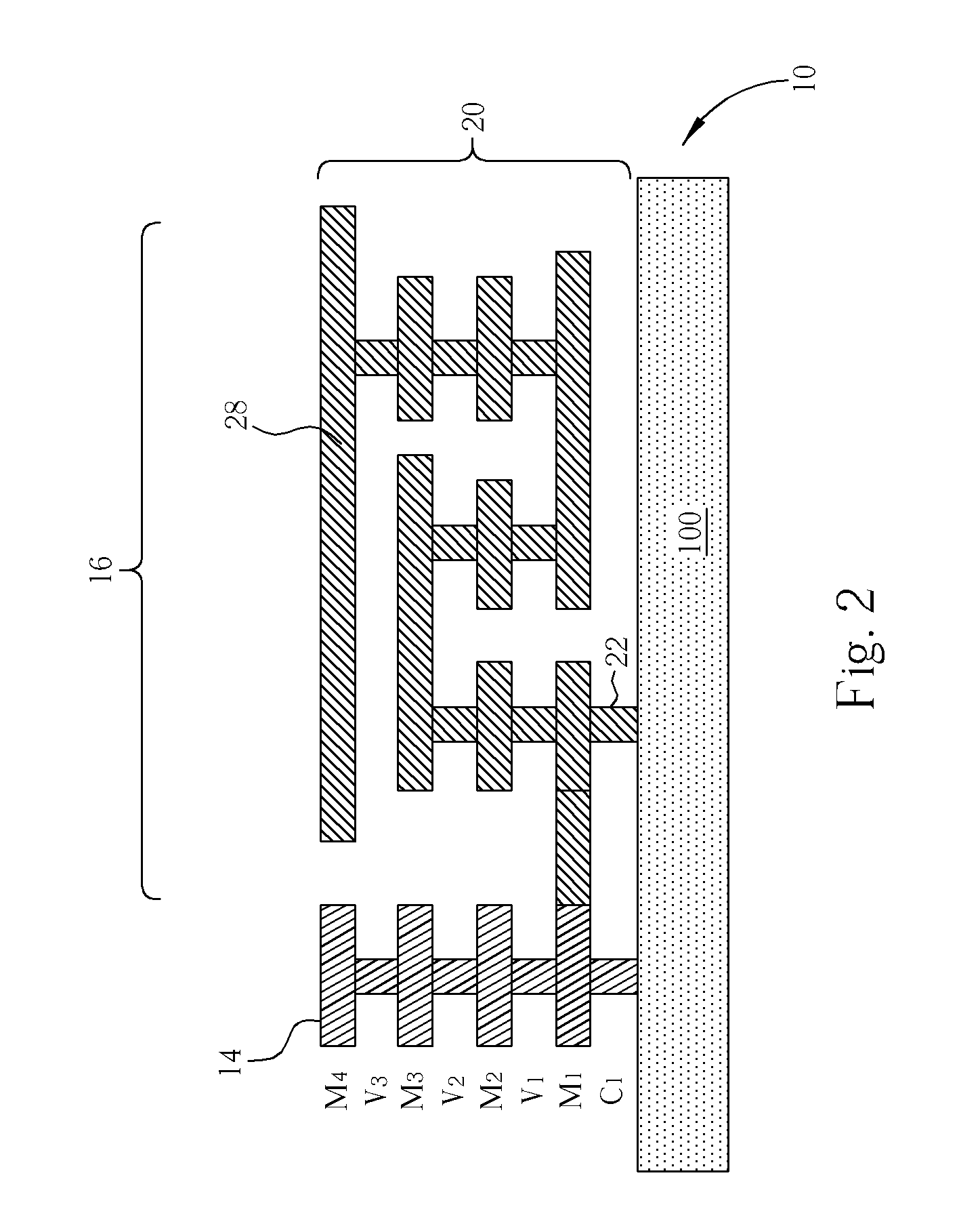
[0018] The present invention is directed to an on-chip test circuit constructed at four vulnerable corners of an integrated circuit chip or die for assessing chip integrity. Interface delamination occurs between low-k dielectric layers during or after the wafer dicing. It has been observed that such interface delamination phenomenon is particularly severe at the four corners of a single die or chip, and the interface delamination even penetrates into the active circuit die area protected by a die seal ring or metallic arrester wall, even in combination with a crack-stopping trench slit disposed along the perimeter of each die.

[0019] It is believed that the severe interface delamination at the four corners of a single die results from mechanical stress created by the cutting blade during the wafer dicing process. During wafer dicing, either in the form of grinding-cutting or scribing, the aforesaid mechanical stress concentrates on the four corners of an active circuit die area, cau...


PUM


Abstract

A semiconductor chip includes an active inner circuit; a die seal ring surrounding the active inner circuit; a first circuit structure fabricated at a first corner of the semiconductor chip outside the die seal ring and electrically connected to the die seal, wherein the first circuit structure has a first solder pad; and a second circuit structure fabricated at a second corner of the semiconductor chip outside the die seal ring and electrically connected to the die seal, wherein the second circuit structure has a second solder pad.

Description

BACKGROUND OF THE INVENTION [0001] 1. Field of the Invention [0002] The present invention relates generally to the reliability test of semiconductor integrated circuit chips and, more particularly, to an on-chip test circuit constructed at corners of an integrated circuit chip or die for assessing chip integrity. [0003] 2. Description of the Prior Art [0004] Semiconductor manufacturers have been shrinking transistor size in integrated circuits (IC) to improve chip performance. This has resulted in increased speed and device density. For sub-micron technology, the RC delay becomes the dominant factor. To facilitate further improvements, semiconductor IC manufacturers have been forced to resort to new materials utilized to reduce the RC delay by either lowering the interconnect wire resistance, or by reducing the capacitance of the inter-layer dielectric (ILD). A significant improvement was achieved by replacing the aluminum (Al) interconnects with copper, which has ˜30% lower resisti...

Claims


Application Information

Patent Timeline
Patent Type & Authority Applications(United States)
IPC IPC(8): H01L23/52
CPCG01R31/2853G01R31/2884H01L2224/13H01L23/585H01L23/562H01L2224/05085H01L2224/05568H01L2224/05001H01L2924/00014H01L24/05H01L24/06H01L24/16H01L2224/05599
Inventor JAO, JUI-MENGKUO, CHIEN-LI
Owner UNITED MICROELECTRONICS CORP
Why Eureka
Try Eureka