Package with solder-filled via holes in molding layers

a technology of soldering holes and molding layers, applied in the field of electronic packages, to achieve the effect of improving configuration and procedur

Inactive Publication Date: 2008-02-14
LIN PAUL T +1
View PDF5 Cites 50 Cited by
  • Summary
  • Abstract
  • Description
  • Claims
  • Application Information

AI Technical Summary

Benefits of technology

[0009]It is therefore an aspect of the present invention to provide an improved configuration and procedure for packaging an integrated circuit (IC) chip and assembling multiple IC packages together as modules by implementing a via-hole ball-grid-array (VHBGA) configuration. The VHBGA is implemented with a leadframe, flexible circuit or PCB type of substrate provided with via holes in the molding layers from the top and the bottom sides of the molded package. These via holes are filled with solder

Problems solved by technology

Due to space limitation for some packages with high input-output (I/O) requirements, the via-holes in the

Method used


Image

  • Package with solder-filled via holes in molding layers
  • Package with solder-filled via holes in molding layers
  • Package with solder-filled via holes in molding layers

Examples


Embodiment Construction

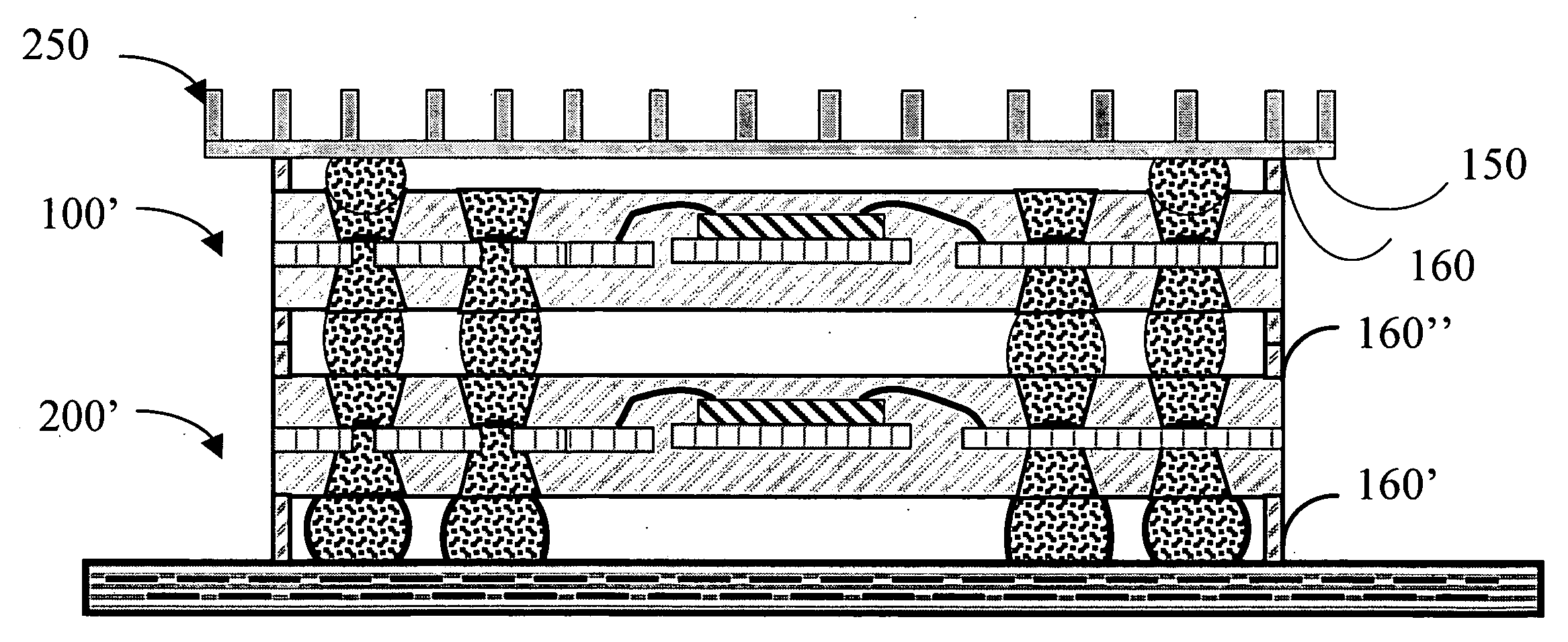
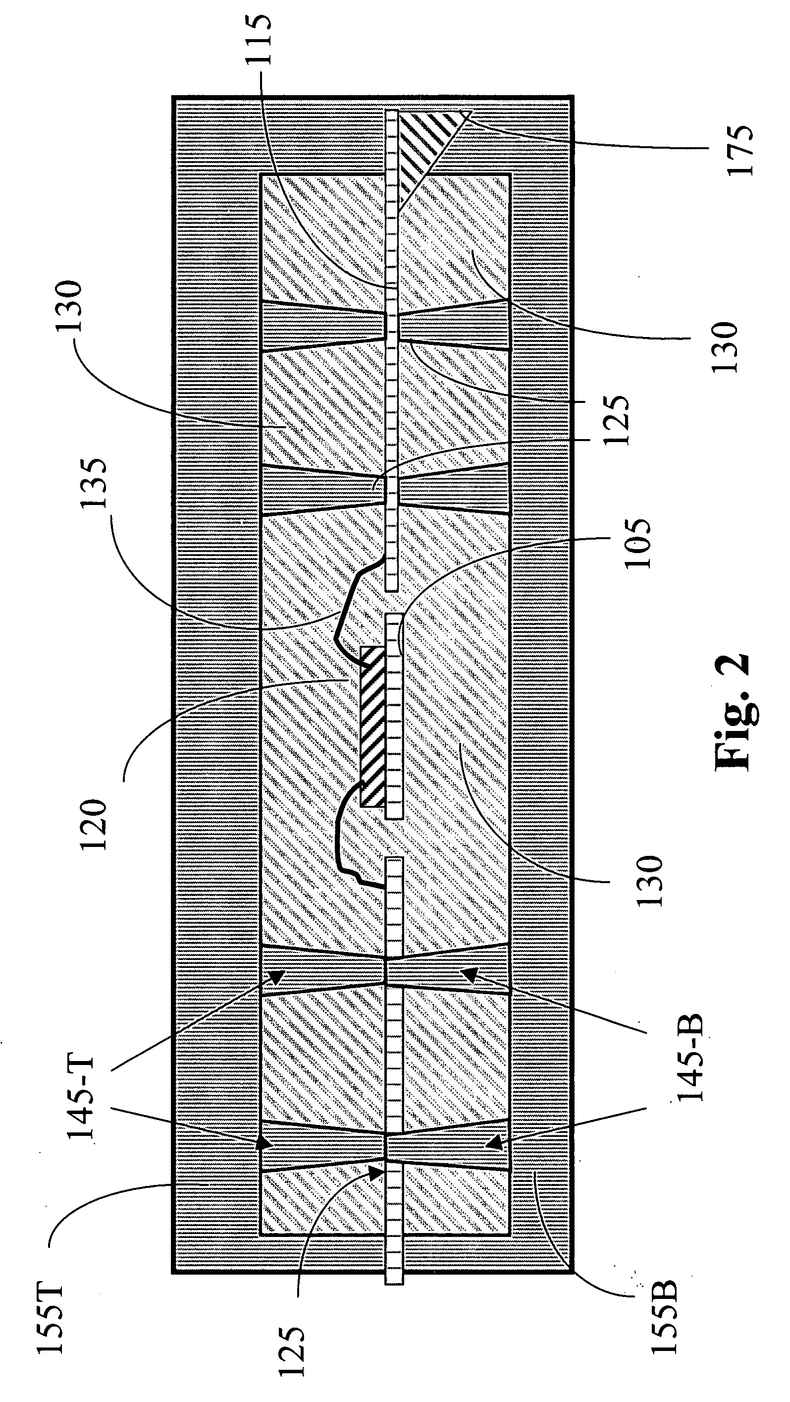
[0028]FIG. 1 shows a top view of a leadframe after the operation of a die bonding to form a molded ball grid array (BGA) package with via holes in the molding layers on both the top and bottom sides of the package according to an exemplary embodiment of this invention. The leadframe includes a peripheral supporting frame 110 with four peripheral frame stripes configured substantially with a square or rectangular shape. The leadframe further includes a plurality of metal lines 115 extended to the peripheral frame 110 from different predefined locations surrounding a central portion 105, which is designated for placement of an integrated circuit (IC) chip 120. Each of these metal lines 115 further includes at least one or several contact pads 125. By applying a wire bonding process, the bonding wires 135 are formed to interconnect the integrated circuit (IC) chip 120 to the bonding wire fingers, which is at the inner end of the metal line 115, and has proper local plating layer to enh...


PUM

PropertyMeasurementUnit
Mechanical strengthaaaaaaaaaa
Flexibilityaaaaaaaaaa
Electrical conductoraaaaaaaaaa

Abstract

The present invention discloses an electronic package to contain and protect an integrated circuit (IC) chip. The electronic package further includes a leadframe, a flexible circuit or PCB type of substrate. The leadframe, flexible circuit or PCB type substrate further includes solder contacts, which are aligned with via holes in the molding layers on the top and bottom sides of the package. These via holes are for placing solder paste or solder balls from above and below for electrical access to the IC chip. These solder balls provide access for electrical testing after the package is mounted on a motherboard. They also provide the connection points for stacking multiple packages vertically.

Description

[0001]This patent application is a Non-Provisional Application and claims the Priority dates of a first Provisional Application 60 / 836,419 on Aug. 8, 2006 and a second Provisional Application 60 / 918,279 filed on Mar. 14, 2007 filed by the Applicants of this Non-Provisional Patent Application.BACKGROUND OF THE INVENTION[0002]1. Field of the Invention[0003]This invention relates generally to the electronic package. More particularly, this invention relates to a package configuration to provide low cost high performance electronic device packages that allows on-board testing and options for attaching electrical shielding, heat spreader or stack of multiple packages for highly integrated portable electronic products.[0004]2. Description of the Prior Art[0005]For conventional molded plastic packages using leadframe for interconnection substrates, packages such as QFP, SOIC, PLCC or SOJ, the IC chip and chip interconnects by either wire bonding or implementing a flip chip configuration, t...

Claims


Application Information

Patent Timeline
IPC IPC(8): H01L23/48B29C45/34H01L23/552H01L21/50
CPCB29C45/0053H01L2924/1815B29C45/2628H01L21/50H01L21/565H01L23/3107H01L23/3128H01L23/552H01L25/105H01L2224/48227H01L2224/48247H01L2224/49171H01L2924/01078H01L2924/14H01L2924/15311H01L2924/15331H01L2924/16152H01L2924/3025H01L24/48H01L24/49B29C45/14655H01L2225/1058H01L2225/1029H01L2924/3511H01L2224/73265H01L2224/32245H01L2924/00H01L2924/00012H01L24/73H01L2924/181H01L2924/19107H01L2924/00014H01L2224/45099H01L2224/45015H01L2924/207
Inventor LIN, PAUL T.CHANG, CHI-SHIH
Owner LIN PAUL T
Why Eureka
Try Eureka