Eureka AIR delivers breakthrough ideas for toughest innovation challenges, trusted by R&D personnel around the world.

Shielded gate trench (SGT) MOSFET cells implemented with a schottky source contact

a source contact and shielded gate technology, applied in the direction of semiconductor devices, diodes, electrical apparatus, etc., can solve the problems of increasing series resistance, increasing the resistance of devices, and reducing the on resistance of devices, so as to improve the area efficiency of the integrated schottky, improve the device performance, and improve the switching performance.

Active Publication Date: 2008-11-18
ALPHA & OMEGA SEMICON LTD
View PDF5 Cites 53 Cited by
  • Summary
  • Abstract
  • Description
  • Claims
  • Application Information

AI Technical Summary

Benefits of technology

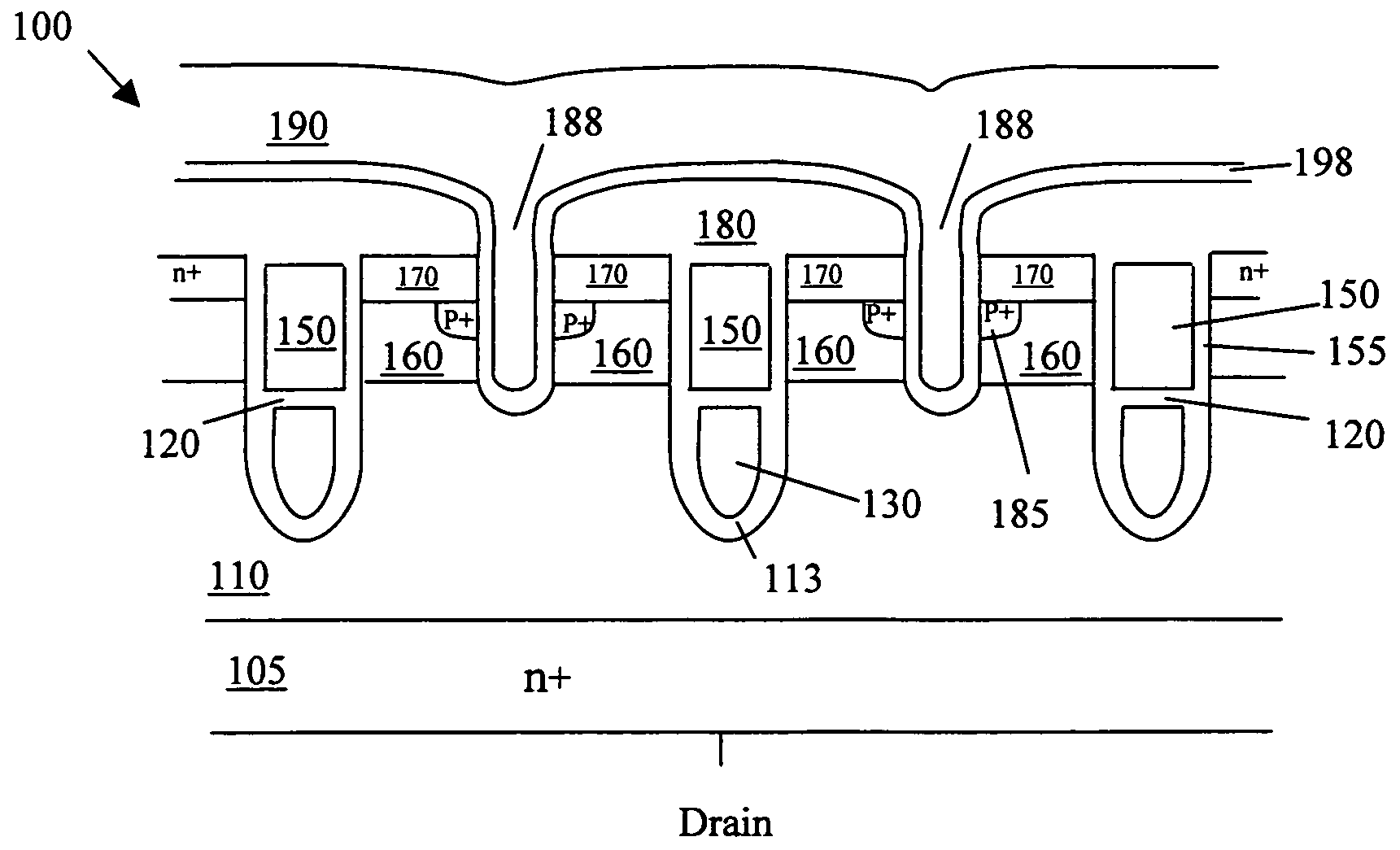
[0015]Another aspect of this invention is to combine the new and improved SGT connections with the integrated Schottky source contact trench configuration to further improve the MOSFET switching performance and improve the area efficiency of the integrated Schottky. A metal layer of low barrier height is formed to cover a source contact trench thus functioning as an integrated Schottky contact to bypass the body diode thus improving the device performance. Meanwhile punch through prevention is provided in the source contact Schottky by forming a punch through implant region disposed along the trench walls.
[0016]Specifically, it is an aspect of the present invention to provide improved SGT device configuration and manufacturing method to reduce the gate to drain capacitance. The device further includes source contact trenches opened through the body region and covered with a low barrier height metal layer such as Ti or TiSi2 layer to function as Schottky barrier diode to bypass the body diode thus improving the behavior of the power MOSFET devices. The devices disclosed in this invention are especially useful for application in H-bridge and synchronous rectification application.
[0017]Briefly in a preferred embodiment this invention discloses a trenched semiconductor power device. The trenched semiconductor power device includes a plurality of interconnected trenches form on a semiconductor substrate. At least one of the interconnected trenches constitutes a shielded gate trench (SGT) for the semiconductor power device. The SGT includes a trenched gate disposed on an upper portion of the SGT and a bottom shielding electrode disposed on a bottom portion of the SGT insulated from the trenched gate. At least one of the interconnected trenches constitutes a source-connecting trench filled with a conductive trench-filling material electrically connected to the bottom shielding electrode of the SGT for electrically connecting to a source metal disposed on top of the source-connecting trench. The trenched semiconductor power device further includes a trenched source contact opened between the gate trenches extended through a source region into a body region for electrically connecting the source region to a source metal disposed on top of the insulation layer. The trenched source contacts further covered with a low barrier height metal layer such as a Ti / TiN or TiSi2 / TiNlayer to function as an integrated Schottky barrier diode in each cell of the power semiconductor device thus improving the device performance. The semiconductor power device further includes a punch through prevention region doped with a body type dopant along trench walls of the source contact trenches for preventing a punch through of the semiconductor power device.
[0018]Another embodiment of this invention includes a shielding structure disposed at the bottom of the trenched gate and insulated from the trenched gate. The shielding structure extends to a depth deeper than the bottom of source contact trench where the Schottky diode is formed. The shielding structure provides shielding effect for the trenched gate thus leading to the reduction of gate drain capacitance Cgd therefore improves the switching speed. The shielding structure further provides shielding effect for the trenched Schottky leading to the reduction of leaking current therefore enable the use of low barrier height material for the Schottky contact to improve the Schottky junction resistance without trading off leaking current that constantly challenging designers while trying to optimize a pair of competing parameter.

Problems solved by technology

However, there is a tradeoff that there is an increase of the series resistance.
However, these devices still have the limitations of using metals of relatively high barrier height.
The device performance cannot satisfy the modern applications that require further reduction of the on resistance and higher drive currents.
However, the high barrier height metal as required to achieve acceptable low leakage current in the off state presents a disadvantage due to the higher costs of depositing both the high barrier height metal and the low barrier height metal to meet the requirements of Schottky and source-body ohmic contact.
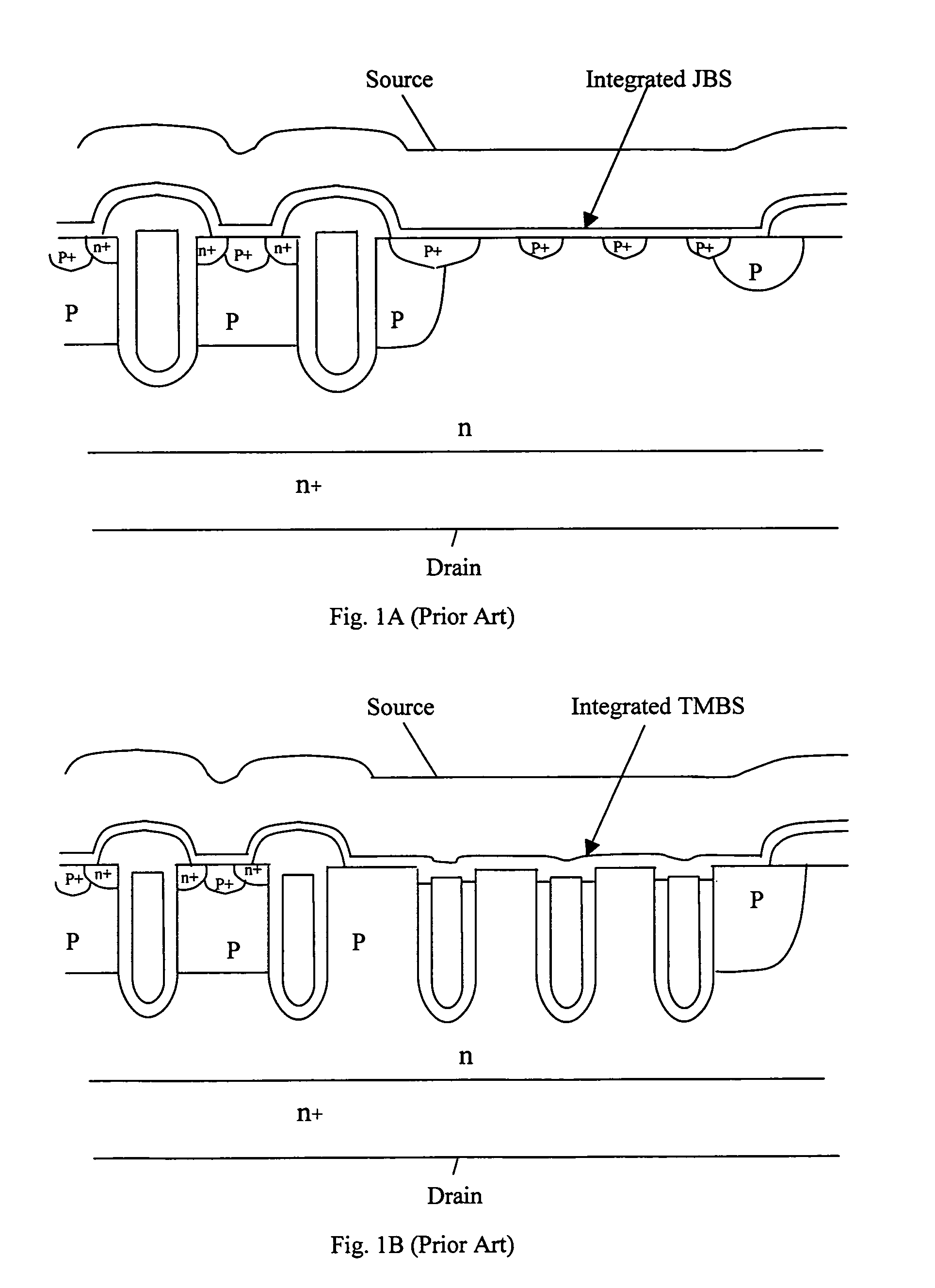
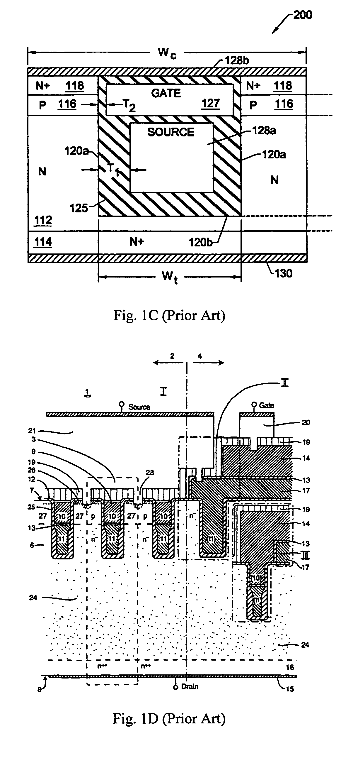
Additionally, the above device configurations as shown in FIGS. 1A, 1B and 2 are still limited by a relatively high gate-to-drain capacitance (Cgd) caused by the coupling between the trenched gate and the drain disposed on the bottom portion of the substrate.
The technologies as disclosed are still confronted with technical limitations and difficulties.
The above patented-disclosures including transistor configurations still have a common difficulty.
This inevitably increases the source electrode resistance.
Furthermore, the extra masks needed to create such connection also increase the cost of manufacturing.

Method used


Image

  • Shielded gate trench (SGT) MOSFET cells implemented with a schottky source contact
  • Shielded gate trench (SGT) MOSFET cells implemented with a schottky source contact
  • Shielded gate trench (SGT) MOSFET cells implemented with a schottky source contact

Examples


Embodiment Construction

[0028]Referring to FIGS. 3A to 3D for a top view and three cross sectional views respectively of a trenched MOSFET device 100 of this invention. As shown in FIG. 3B, the trenched MOSFET device 100 is supported on a substrate 105 formed with an epitaxial layer 110. The trenched MOSFET device 100 includes a shielded gate trench (SGT) structure. The SGT structure includes a bottom shielding electrode 130 insulated from and disposed below a trenched gate 150. The bottom SGT structure 130 filled with a polysilicon therein is provided to shield the trenched gate 150 from the drain disposed below the trench bottom. The bottom SGT structure 130 is insulated from the drain region by a dielectric layer 113. An insulation layer 120 separates the bottom shielding electrode 130 from the trenched gate 150. The trenched gate 150 includes polysilicon filling in a trench surrounded with a gate insulation layer 155 covering the trenched walls. A body region 160 that is doped with a dopant of second c...


PUM


Abstract

This invention discloses a semiconductor power device that includes a plurality of power transistor cells surrounded by a trench opened in a semiconductor substrate. At least one active cell further includes a trenched source contact opened between the trenches wherein the trenched source contact opened through a source region into a body region for electrically connecting the source region to a source metal disposed on top of an insulation layer wherein a trench bottom surface of the trenched source contact further covered with a conductive material to function as an integrated Schottky barrier diode in said active cell. A shielding structure is disposed at the bottom and insulated from the trenched gate to provide shielding effect for both the trenched gate and the Schottky diode.

Description

[0001]This Patent Application is a Continuation in Part (CIP) Application of Ser. No. 11 / 056,346 (issued into U.S. Pat. No. 7,285,822 on Oct. 23, 2007) filed by a common Inventor of this Application on Feb. 11, 2005. The Disclosures made in that Application is hereby incorporated by reference.BACKGROUND OF THE INVENTION[0002]1. Field of the Invention[0003]The invention relates generally to the semiconductor power devices. More particularly, this invention relates to an improved and novel manufacturing process and device configuration for providing the MOSFET device with shielded trench gates with cells provided with Schottky source contact for improving performance of high frequency power switching, H-bridge and synchronization rectification applications.[0004]2. Description of the Related Art[0005]In order to reduce the power consumptions and to increase the switching speed of a power semiconductor power device, it is desirable to further reduce the on-resistance and the gate capac...

Claims


Application Information

Patent Timeline
Patent Type & Authority Patents(United States)
IPC IPC(8): H01L29/94
CPCH01L29/407H01L29/7813H01L29/66727H01L29/66734H01L29/7806H01L29/7811H01L29/0615H01L29/0623H01L29/0696H01L29/1095H01L29/41741H01L29/42368H01L29/41766
Inventor BHALLA, ANUPLUI, SIK K.
Owner ALPHA & OMEGA SEMICON LTD
Why Eureka
Eureka Blog
Learn More