
Photonically tuned etchant reactivity for wet etching

a technology of wet etching and etching rate, which is applied in the direction of photomechanical equipment, photosensitive material processing, instruments, etc., can solve the problems of unstable etching, yield loss or degradation of device performance, and non-uniform etching rate, and achieve the effect of expanding the range of etching behavior

Active Publication Date: 2020-03-05
TOKYO ELECTRON LTD
View PDF0 Cites 0 Cited by
  • Summary
  • Abstract
  • Description
  • Claims
  • Application Information

AI Technical Summary

Benefits of technology

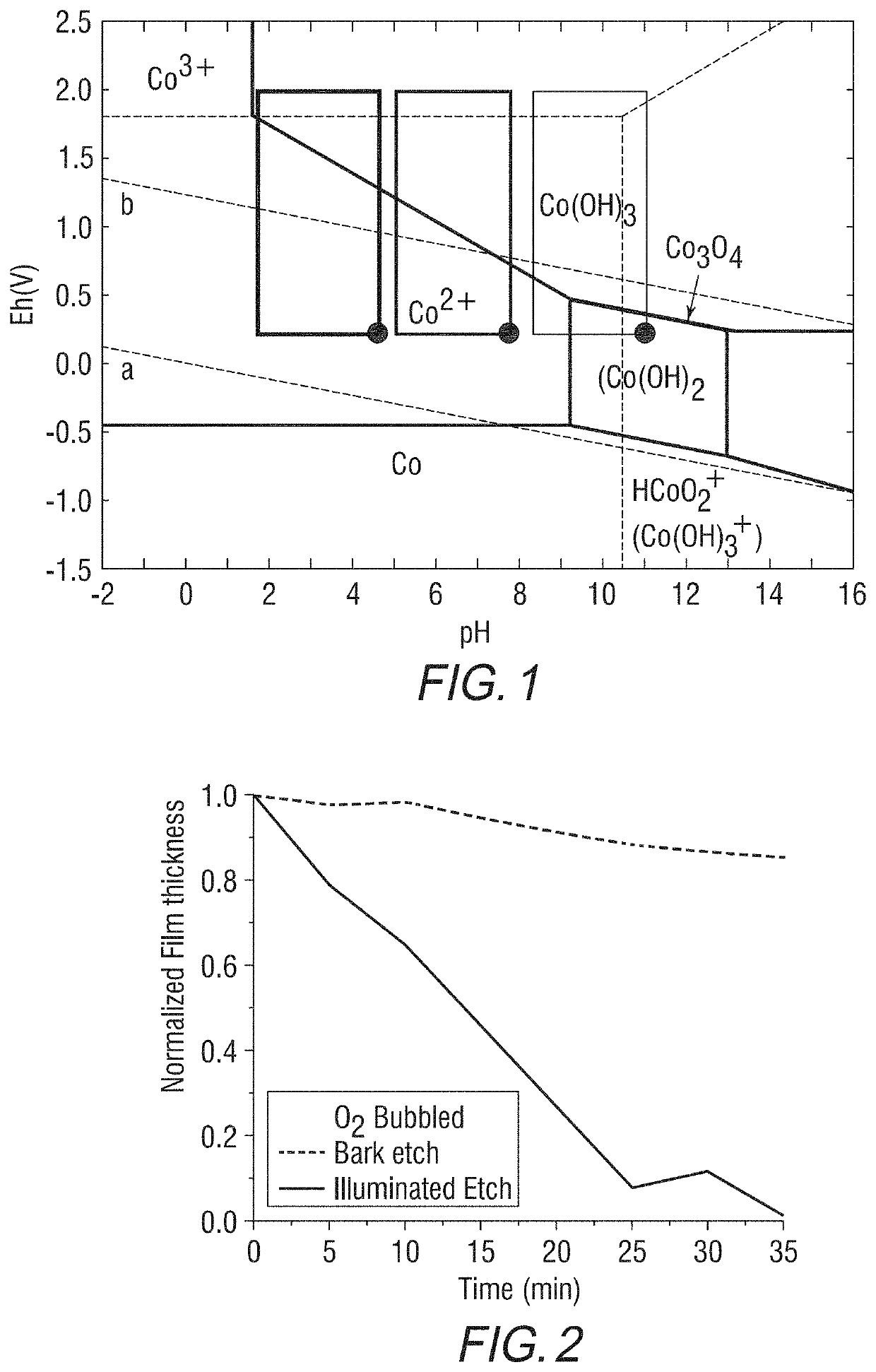
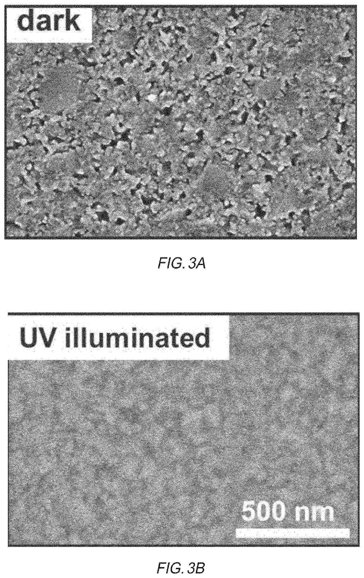
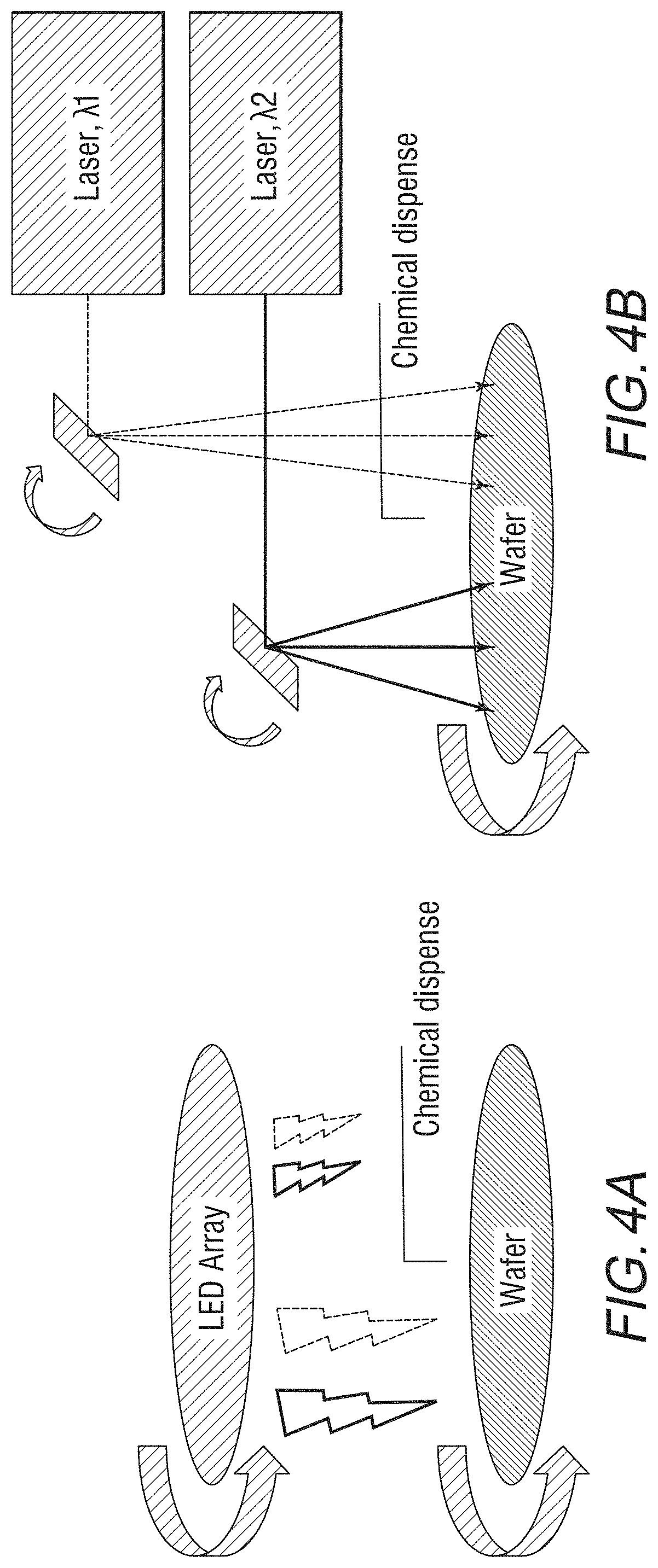
This patent describes a method to adjust the etch rate of liquid solutions using spatial resolution on the wafer to correct for non-uniformities in etchant composition and temperature over the surface of the wafer. The method involves adding photoactive components to the etch solution which can adjust the pH and oxidation potential of the solution under illumination. This technique greatly expands a range of etch behaviors that can be achieved with a single solution and compensates for temperature variations across the wafer. The method also allows for temporal and spatial control of etch rate on a wafer and improves wet etch processes. The etchant becomes more reactive under illumination with particular wavelengths and can be stored in a less reactive state to be more stable.

Problems solved by technology

Additionally, non-uniformities in etchant composition and temperature over the surface of the wafer can cause non-uniformities in etch rate.
Such non-uniform etching can lead to yield losses or degradation in device performance.
In many processes, compositions and temperatures required to achieve a desired etch behavior cause the etchants to become unstable.
To control these processes, the etchant can be formulated immediately before use, which increases costs.
During dispense there are other challenges.
When etch rates have a strong temperature dependence, then the etch rate will decrease towards the edge of the wafer resulting in non-uniform etching.

Method used


Image

  • Photonically tuned etchant reactivity for wet etching
  • Photonically tuned etchant reactivity for wet etching
  • Photonically tuned etchant reactivity for wet etching

Examples


Embodiment Construction

[0018]Reference throughout this specification to “one embodiment” or “an embodiment” means that a particular feature, structure, material, or characteristic described in connection with the embodiment is included in at least one embodiment of the application, but do not denote that they are present in every embodiment. Thus, the appearances of the phrases “in one embodiment” or “in an embodiment” in various places throughout this specification are not necessarily referring to the same embodiment of the application. Furthermore, the particular features, structures, materials, or characteristics may be combined in any suitable manner in one or more embodiments.

[0019]Conventional wet etch solutions typically have a set reactivity and etch rate for a given material based on the composition and temperature of the solution. Techniques herein, however, provide methods and systems to adjust the etch rate of a solution of a given composition at a given temperature in real time. Additionally,...


PUM


Abstract

A method and a system for etching of semiconductor substrates, and particularly, wet etching of wafers. The etch rate of liquid solutions applied on the wafer is adjusted by irradiating the liquid solutions with spatially varied light intensity. Photo-reactive agents are added to the liquid solutions, the agents including photo acids, photo bases and photo-oxidizers. Illumination of the photo-reactive agents causes increase / decrease of the pH value and oxidation potential value of the liquid solutions.

Description

CROSS REFERENCE TO RELATED APPLICATIONS[0001]This application is based on and claims the benefit of and priority to U.S. Provisional Patent Application No. 62 / 726,603, entitled “PHOTONICALLY TUNED ETCHANT REACTIVITY FOR WET ETCHING”, filed on Sep. 4, 2018, the entire contents of which are herein incorporated by reference.BACKGROUNDTechnical Field[0002]The present application relates to etching of semiconductor substrates, and particularly to wet etching of wafers. More particularly, it relates to a method and a system for adjusting an etch rate of liquid solutions applied on the wafer by irradiating the liquid solutions with spatially varied light intensity.Description of the Related Art[0003]Semiconductor fabrication involves many different steps of depositing, growing, patterning, removal, and cleaning of wafers. Various different materials are added and removed or partially removed, while other materials remain. One removal technique is that of wet etching. Wet etching typically ...

Claims


Application Information

Patent Timeline
IPC IPC(8): H01L21/67G03F7/004G03F7/42
CPCG03F7/425G03F7/0041H01L21/67075G03F7/423G03F7/40H01L21/32134H01L21/30604H01L21/31111H01S3/0007H01L21/67057H01L2924/40402
Inventor ABEL, PAULZANDI, OMID
Owner TOKYO ELECTRON LTD
Learn More