Sliding test device for electronic components

a test device and electronic component technology, applied in the direction of measurement devices, testing/measuring connectors, instruments, etc., can solve the problems of large volume occupied, complicated structure of above-mentioned conventional testing apparatus, and disadvantageous space arrangement of test areas, so as to improve the stability and service life of the device, the effect of reducing the volume occupied by the devi

Active Publication Date: 2020-03-12
CHROMA ATE
View PDF0 Cites 3 Cited by
  • Summary
  • Abstract
  • Description
  • Claims
  • Application Information

AI Technical Summary

Benefits of technology

[0007]The main object of the present invention is to provide a sliding test device for electronic components, which is not only capable of effectively reducing the volume occupied by the device and thus allowing more test device to be arranged in the test area, but also capable of providing a pressing force sufficient to ensure contact between test probes and contacts of a chip and withstanding a reaction force for internal force balance so as to improve the stability and service life of the device.

Problems solved by technology

However, a test arm of an existing testing apparatus such as a test arm TR shown in FIG. 8 (reproduced from FIG. 1A of Taiwanese Patent No. 1452310 entitled “TESTING DEVICE FOR STACKED CHIPS”), is bulky, especially in the vertical direction and thus is disadvantageous for the space arrangement of a test area.
However, the above-mentioned conventional testing apparatus has a complicated structure and a considerable volume occupied.

Method used


Image

  • Sliding test device for electronic components
  • Sliding test device for electronic components
  • Sliding test device for electronic components

Examples


first embodiment

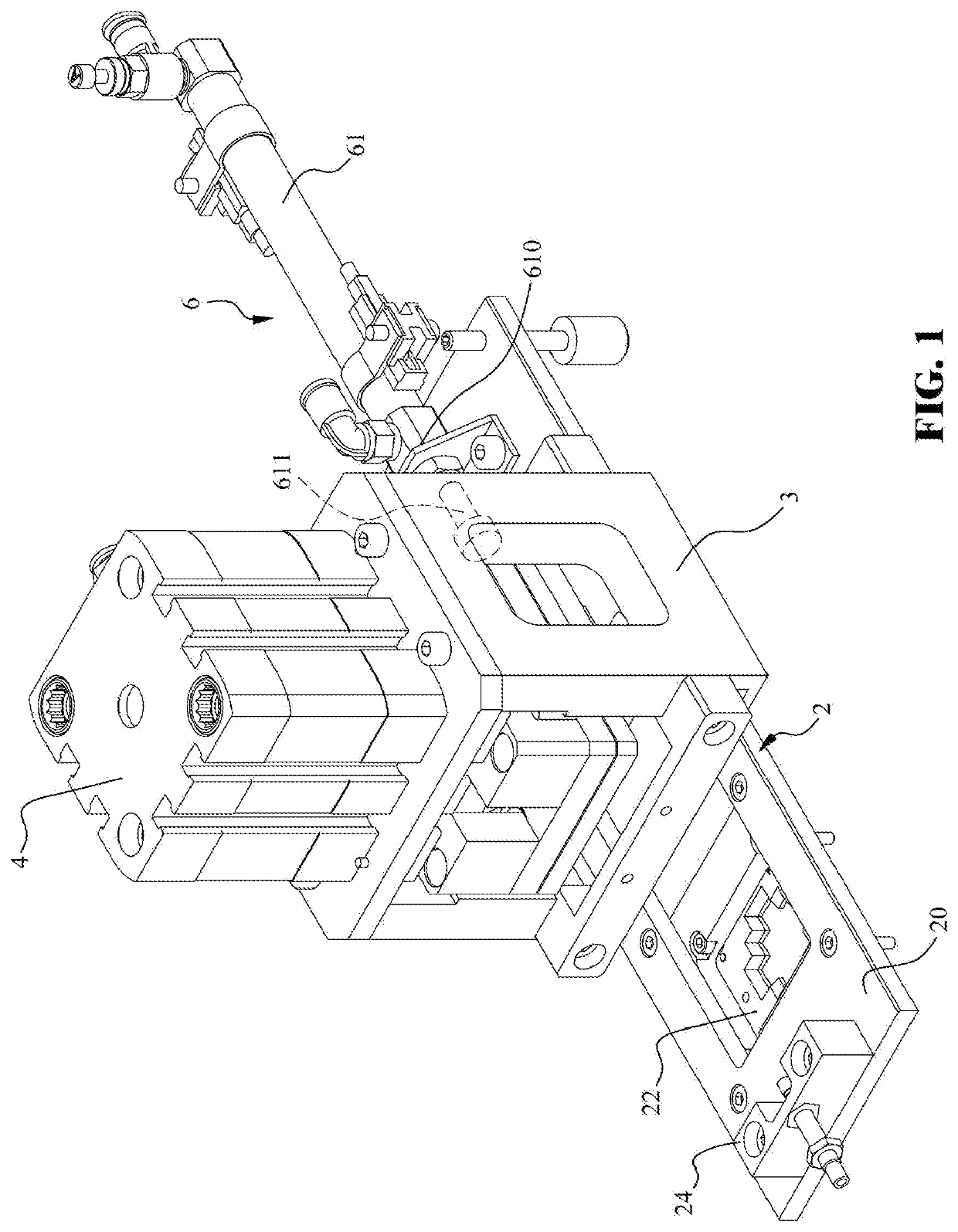
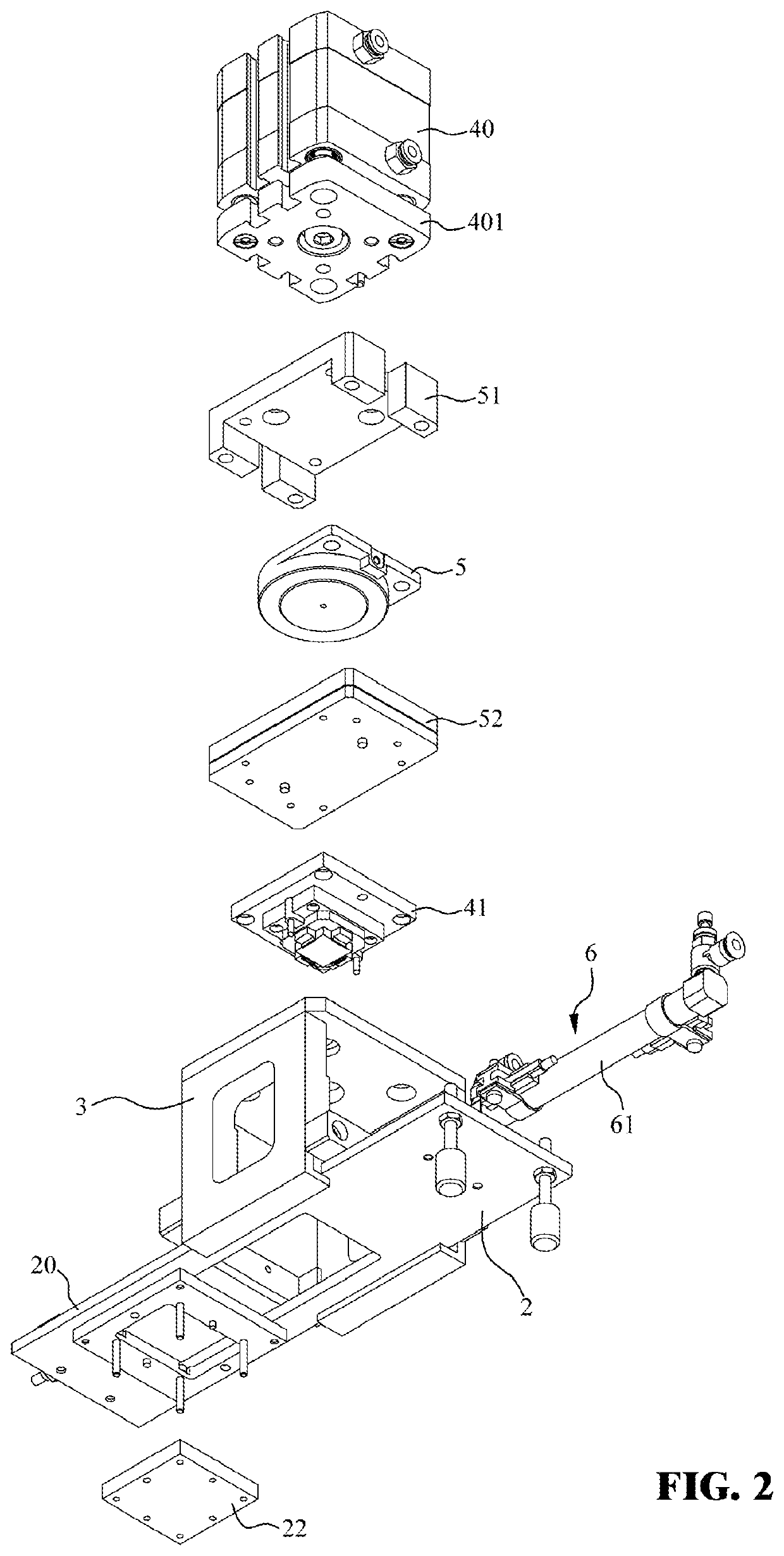
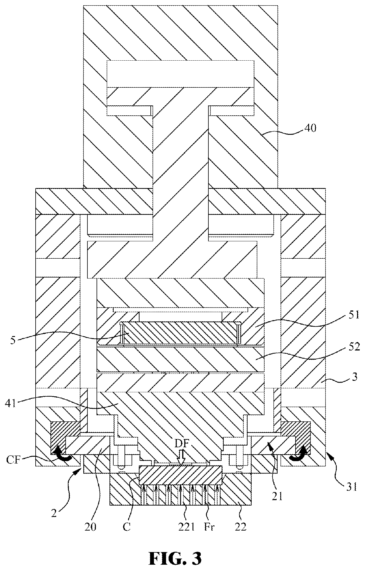
[0028]The sliding frame 3 of the first embodiment is a rectangular frame, and two lateral edges of the sliding frame 3 to be coupled to the base 2 each are provided with a second sliding guide 31 which is in form of a guide channel. Accordingly, the second sliding guide 31 of the sliding frame 3 in form of the guide groove is slidably engaged with the first sliding guide 21 of the base 2 in form of the guide rail, so that the sliding frame 3 is slidably movable on the base 2.

[0029]The pressing member 4 of the first embodiment includes a vertical linear actuator 40 and a pressing block 41. The vertical linear actuator 40 is a double-acting pneumatic cylinder which is disposed above the sliding block 3, and the piston end 401 of the double-acting pneumatic cylinder is connected to a fixing frame 51 which is U-shaped. The pressing force generating member 5 which is in form a thin diaphragm cylinder is fixed within the fixing frame 51. A force spreading plate 52 is provided beneath the ...

second embodiment

[0035]Actuation of the electric motors 621 causes rotation of the gears 622 so that the sliding frame 3 is slidably moved with respect to the base 2. In another embodiment of the present invention, the gear 622 may be coupled to the electric motor 621 through a speed reducer. In still another embodiment, the plurality of gears 622 can be driven by a single electric motor 621 if a transmission gear set is arranged to couple the plurality of gears 622. In the present invention, the electric motors 621 and the gears 622 are disposed on the sliding frame 3, and the racks 623 are disposed on the base 2. However, in another embodiment of the present invention, the racks can be disposed on the sliding frame 3, and the electric motors and the gears are disposed on the base 2.

[0036]Reference is made to FIG. 5 which is a schematic top view of a third embodiment of the present invention. The main difference between the third embodiment and the first and second embodiments lies in the actuating...


PUM


Abstract

The invention relates to a sliding test device for electronic components, which mainly comprises a base, a sliding frame and a pressing member, wherein an electronic component to be tested is placed in a chip receiving module of the base, and the sliding frame is slidably moved with respect to the base under sliding engagement between a first sliding guide and a second sliding guide so that a pressing block of the pressing member is aligned with the electronic component presses the electronic component. According to the present invention, the pressing member presses the electronic component and exerts a sufficient contact force on the electronic component, and a reaction force caused by the contact force and the elastic restoring force of probes is internally balanced in the device.

Description

BACKGROUND OF THE INVENTIONField of the Invention[0001]The present invention relates to a sliding test device for electronic components and particularly suitable for testing an electronic component by pressing the electronic component onto a test jig.DESCRIPTION OF THE RELATED ART[0002]Generally, in order to test an electronic component, the electronic component to be tested must be placed in a test socket, and then a test arm (a pressing member) is provided to exert a force onto the electronic component and press the electronic component downwardly. This ensures that contacts on a lower surface of the electronic component are entirely and electrically contacted with probes in the test socket and the test accuracy is prevented from being affected by contact failure. However, a test arm of an existing testing apparatus such as a test arm TR shown in FIG. 8 (reproduced from FIG. 1A of Taiwanese Patent No. 1452310 entitled “TESTING DEVICE FOR STACKED CHIPS”), is bulky, especially in th...

Claims


Application Information

Patent Timeline
Patent Type & Authority Applications(United States)
IPC IPC(8): G01R31/28G01R1/04
CPCH01R2201/20G01R31/2887G01R31/2891G01R1/04G01R31/2893G01R1/0408
Inventor OUYANG, CHIN-YICHEN, CHIEN-MINGLU, MENG-KUNG
Owner CHROMA ATE
Why Eureka
Try Eureka