Semiconductor module

Active Publication Date: 2020-03-19
FUJI ELECTRIC CO LTD
View PDF0 Cites 2 Cited by
  • Summary
  • Abstract
  • Description
  • Claims
  • Application Information

AI Technical Summary

Benefits of technology

The present invention aims to provide a semiconductor module that is smaller and has better heat dissipation efficiency. The invention achieves this by improving the design and structure of the semiconductor module. These improvements make it possible to create a smaller semiconductor module that can manage heat better, leading to improved performance and reliability.

Problems solved by technology

Furthermore, there are constraints on the arrangement and orientation of the power semiconductor elements on the conductor foil on the upper surface side of the first circuit substrate, and thus it is difficult to improve the heat dissipation efficiency of heat generated by the power semiconductor elements.

Method used


Image

  • Semiconductor module
  • Semiconductor module
  • Semiconductor module

Examples


embodiment 1

[0041](Configuration of Semiconductor Module)

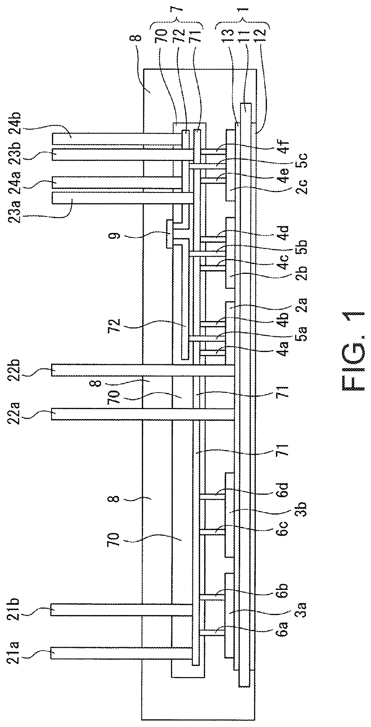
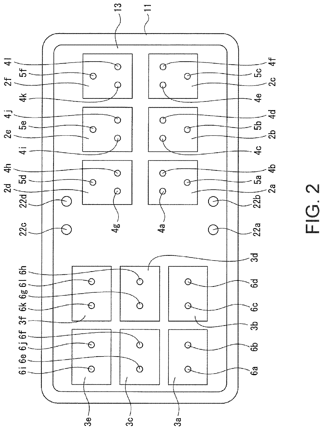
[0042]A 1-in-1 type semiconductor module that forms a part of a half-bridge circuit is illustratively shown as the semiconductor module according to Embodiment 1 of the present invention. FIG. 1 is a side view of the semiconductor module according to Embodiment 1 of the present invention, and FIG. 2 is a top view of the semiconductor module according to Embodiment 1 of the present invention of a first circuit substrate 1 and semiconductor elements (semiconductor chips) 2a to 2f and 3a to 3f seen from above while omitting a second circuit substrate 7 and a sealing material 8. The side view of the semiconductor module seen from the lower side of FIG. 2 corresponds to FIG. 1.

[0043]As shown in FIG. 1 and FIG. 2, the semiconductor module according to Embodiment 1 of the present invention includes: the first circuit substrate 1; the semiconductor elements 2a, 2b, 2c, 2d, 2e, 2f, 3a, 3b, 3c, 3d, 3e, 3f disposed on the first circuit substrate 1; ...

modification example 1

[0095]As shown in FIG. 12, the semiconductor module according to Modification Example 1 of Embodiment 1 of the present invention differs from the semiconductor module according to Embodiment 1 of the present invention in that the resistor element 9 is not disposed on the insulating Layla 70 on the upper surface side of the second circuit substrate 7. When the resistor element 9 is not disposed, the first wiring part 72a and the second wiring part 72b may be directly connected without using the resistor element 9 in the planar pattern of the control wiring layer 72 shown in FIG. 4. Instead of disposing the resistor element 9 on the insulating layer 70 on the upper surface side of the second circuit substrate 7, the resistor element may be embedded inside the insulating layer 70, which can suppress thickness more than if the resistor were disposed on the insulating layer 70.

modification example 2

[0096]As shown in FIG. 13, the semiconductor module according to Modification Example 2 of Embodiment 1 of the present invention differs from the semiconductor module according to Embodiment 1 of the present invention in that the sealing material 8 is disposed so as to expose the upper surface of the insulating layer 70 of the second circuit substrate 7. The exposed upper surface of the insulating layer 70 may have a cooler or other component or the like mounted thereon, for example. Modification Example 2 of Embodiment 1 of the present invention makes it possible to also perform cooling from the upper surface side of the insulating layer 70 of the second circuit substrate 7 and to improve heat dissipation efficiency.


PUM


Abstract

A semiconductor module includes: a first circuit substrate having a conductive layer disposed on an insulating plate; a plurality of semiconductor elements on the conductive layer, a second circuit substrate disposed above the semiconductor elements, the second circuit substrate having a main current wiring layer and a control wiring layer positioned in a layer above the main current wiring layer; a first lead terminal vertically extending upwards from and in contact with the main current wiring layer; a second lead terminal vertically extending upwards from and in contact with the conductive layer of the first circuit substrate; a third lead terminal vertically extending upwards from and in contact with the control wiring layer; and a sealing material covering at least some of the elements mentioned above.

Description

BACKGROUND OF THE INVENTIONTechnical Field[0001]The present invention relates to a semiconductor module on which a plurality of semiconductor elements are mounted.Background Art[0002]A semiconductor module is conventionally known in which a plurality of power semiconductor elements are mounted on the upper surface side of an insulating substrate (first circuit substrate) that is obtained by forming conductor foil on the upper and lower surfaces of a ceramic plate. In this semiconductor module, a circuit substrate (second circuit substrate) in which pins are inserted is used to electrically connect first main electrodes and control electrodes on the upper surface side of power semiconductor elements with the conductor foil on the upper surface side of the first circuit substrate. Lead terminals for connecting to outside are connected to the conductor foil on the upper surface side of the first circuit substrate. The power semiconductor elements are sealed by a sealing material.[0003]...

Claims


Application Information

Patent Timeline
IPC IPC(8): H01L25/18H01L23/538H01L25/07H01L23/31H01L25/16H01L49/02H01L21/48H01L21/56H01L25/00G01R19/00
CPCH01L25/072H01L28/20H01L25/16H01L23/5386H01L21/4853H01L25/18H01L23/3121H01L25/50G01R19/0092H01L21/565H01L23/3735H01L23/5385H01L23/49811H01L2224/32225
Inventor TANIGUCHI, KATSUMI
Owner FUJI ELECTRIC CO LTD
Why Eureka
Try Eureka