PCB panel, pcb, and manufacturing method
a manufacturing method and technology of pcb, applied in the direction of printed circuit parts, printed circuit non-printed electric components association, final product manufacturing, etc., can solve the problems of pcb damage, pcb deformation, and electrical connection breakag
- Summary
- Abstract
- Description
- Claims
- Application Information
AI Technical Summary
Benefits of technology
Problems solved by technology
Method used
Image

Examples
Embodiment Construction
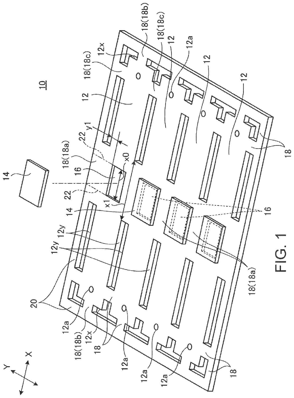
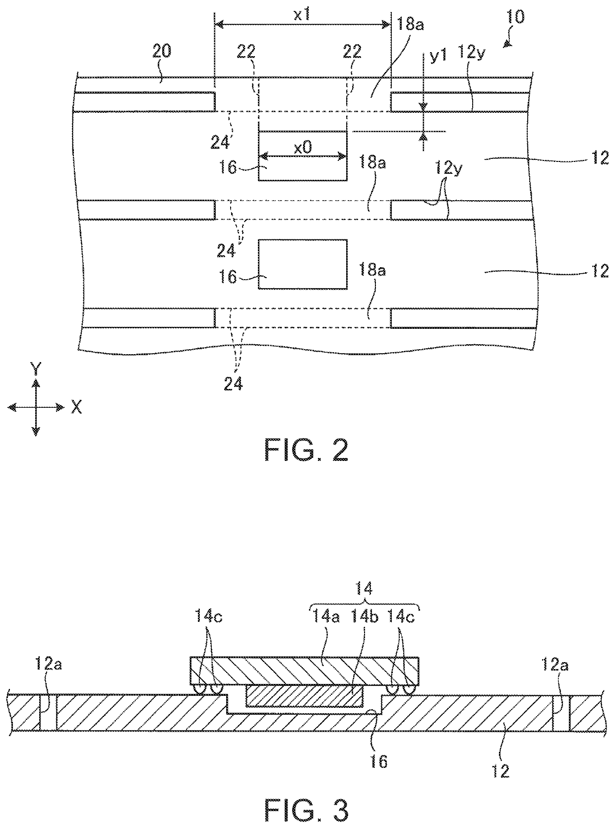
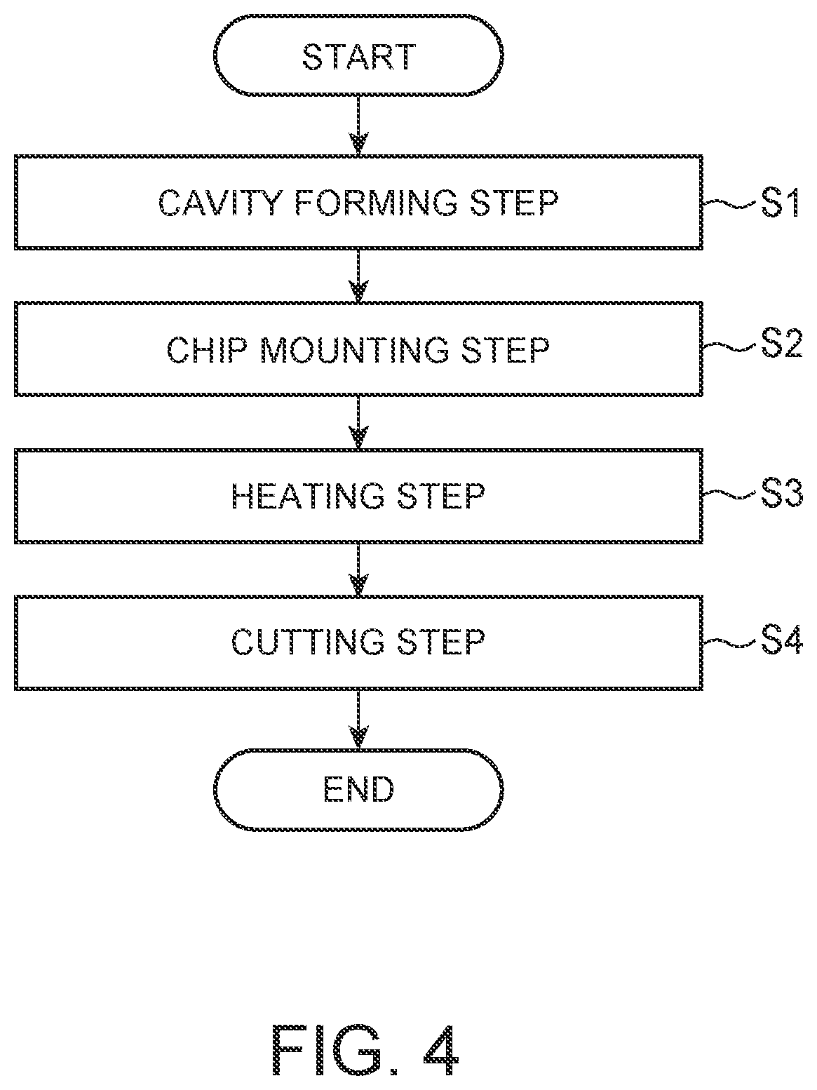
[0017]When PCBs are mass-produced, in some cases, a plurality of PCBs are manufactured from a single panel for the purpose of efficient manufacture. As illustrated in FIG. 8, for example, a plurality of PCBs may be formed on a panel. The PCBs may be connected to frame bodies or other adjacent PCBs by a plurality of stays. Bottomed cavities are formed in the PCBs, and components are mounted in the cavities. After the components are mounted, the components are subjected to a heating process and then soldered. Further, the stays are separated off, and the PCBs are obtained. Each of the PCBs may have, for example, a rectangular shape that is long in an X-direction and short in a Y-direction.
[0018]Meanwhile, the PCBs are required to be even shorter in the Y-direction to make the PCBs smaller. This will cause a dimension y1 between each of the cavities and a Y-direction end to be considerably smaller. If the heating process is carried out in this state, then the cavity and the area around...
PUM
 Abstract
Description
Claims
Application Information
 - R&D
- Intellectual Property
- Life Sciences
- Materials
- Tech Scout
- Unparalleled Data Quality
- Higher Quality Content
- 60% Fewer Hallucinations
Browse by: Latest US Patents, China's latest patents, Technical Efficacy Thesaurus, Application Domain, Technology Topic, Popular Technical Reports.
© 2025 PatSnap. All rights reserved.Legal|Privacy policy|Modern Slavery Act Transparency Statement|Sitemap|About US| Contact US: help@patsnap.com