
Flexible OLED device and method for manufacturing same

a flexible, oled technology, applied in the field of display technology, can solve the problems of oled devices being prone to flow outward, oled devices are sensitive to water and oxygen, metal electrodes and organic light-emitting materials disposed in oled devices are likely to age more quickly, etc., to achieve the effect of increasing the stability and lifetime of oled devices

Inactive Publication Date: 2020-04-23
WUHAN CHINA STAR OPTOELECTRONICS SEMICON DISPLAY TECH CO LTD
View PDF0 Cites 2 Cited by
  • Summary
  • Abstract
  • Description
  • Claims
  • Application Information

AI Technical Summary

Benefits of technology

The present invention provides a flexible OLED device and a method for manufacturing it that increases its stability and lifetime. This is achieved by improving the conventional encapsulation structure and method, which prevents water and oxygen from reaching the organic light-emitting materials and avoids the organic layer outward-flowing problem.

Problems solved by technology

Nevertheless, OLED devices are sensitive to water and oxygen.
In particular, metal electrodes and organic light-emitting materials disposed in OLED devices are likely to age more quickly if being contacted by water or oxygen.
However, organic film in the stacked encapsulation structure is so flowable that it is liable to flow outward to outer boundary of display area.
If organic film flows to exceed beyond the region where inorganic film is formed, water and oxygen would easily enter into OLED devices in lateral direction, thus damaging OLED devices.

Method used


Image

  • Flexible OLED device and method for manufacturing same
  • Flexible OLED device and method for manufacturing same

Examples


Embodiment Construction

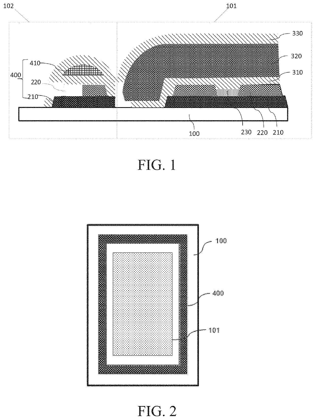
[0059]The following embodiments refer to the accompanying drawings for exemplifying specific implementable embodiments of the present disclosure. Moreover, directional terms described by the present disclosure, such as upper, lower, front, back, left, right, inner, outer, side, etc., are only directions by referring to the accompanying drawings, and thus the used directional terms are used to describe and understand the present disclosure, but the present disclosure is not limited thereto. In the drawings, the same reference symbol represents the same or similar components.

[0060]Please refer to FIG. 1, which is a schematic diagram showing a structure of a flexible organic light-emitting diode (OLED) device according to one embodiment of the present disclosure.

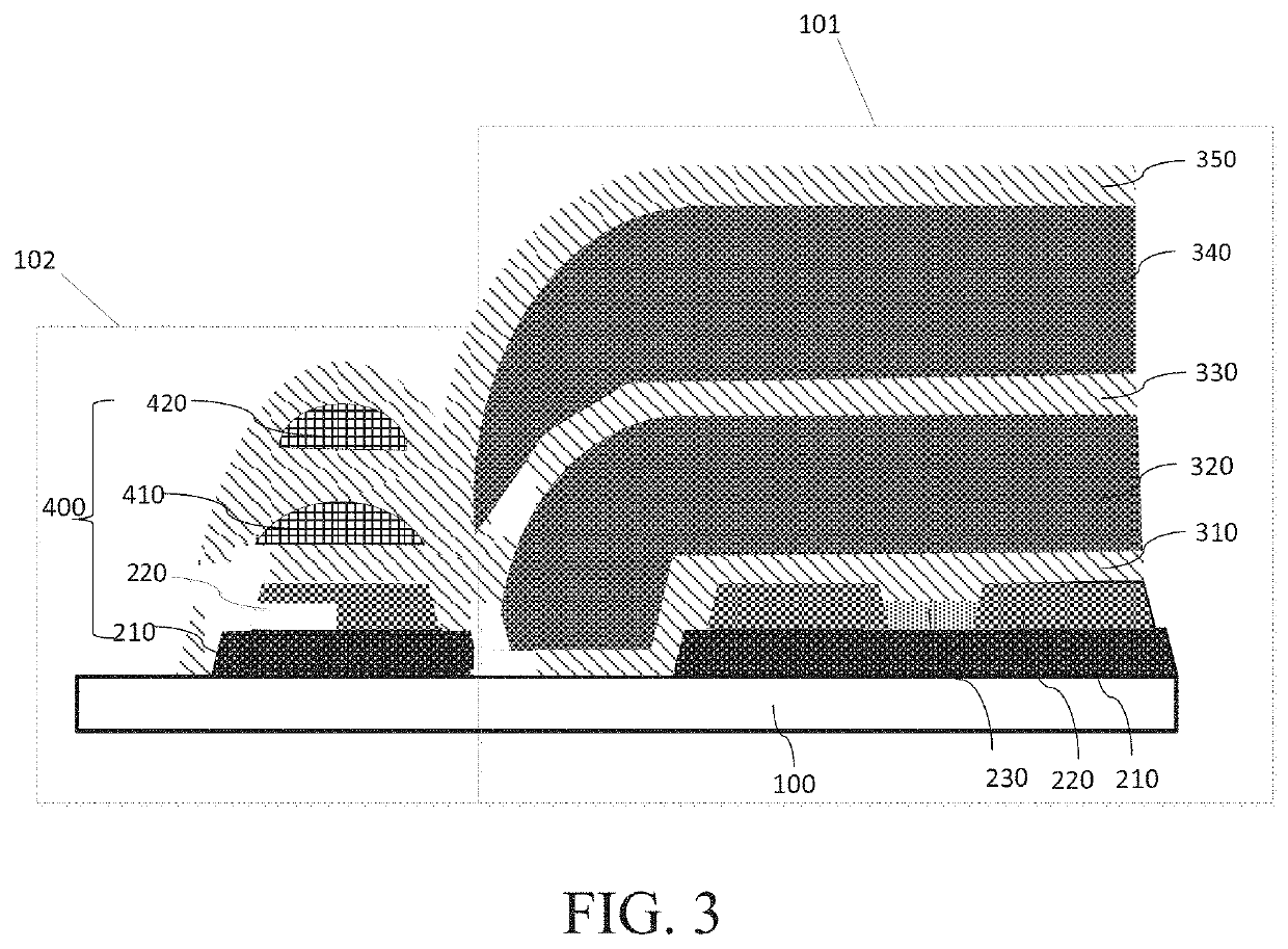
[0061]As shown in FIG. 1, the flexible OLED device includes a display area 101 and a non-display area 102. The flexible OLED device includes a flexible substrate 100, a planarization layer 210, a pixel defining layer 220 and an...


PUM

PropertyMeasurementUnit
flexibleaaaaaaaaaa
areaaaaaaaaaaa
flexibilityaaaaaaaaaa

Abstract

The present disclosure provides a flexible organic light-emitting diode (OLED) device and a method for manufacturing same. The flexible OLED device includes a pixel defining layer disposed on the planarization layer within a portion of a display area and on the planarization layer within a non-display area, a first inorganic layer disposed on the pixel defining layer, a first barrier layer disposed on the first inorganic layer within the non-display area, a first organic layer disposed on the first inorganic layer within the display area, and a second inorganic layer disposed on the first barrier layer and the first organic layer.

Description

FIELD OF INVENTION[0001]The present disclosure relates to the field of display technology, and more particularly to a flexible OLED device and a method for manufacturing the same.BACKGROUND[0002]In the field of flat panel displays, TFT-LCDs have a majority of display market owing to its mature technique, and because they could be stably mass produced. Compared to LCDs, organic light-emitting diode (OLED) devices possess outstanding properties, including being self-illuminating, having low power consumption, and being flexible, and thus are considered as new generation display technique that could be used in various products.[0003]Nevertheless, OLED devices are sensitive to water and oxygen. In particular, metal electrodes and organic light-emitting materials disposed in OLED devices are likely to age more quickly if being contacted by water or oxygen. In order to prevent them from being damaged and protect the same, metal electrodes and organic light-emitting materials are required ...

Claims


Application Information

Patent Timeline
Patent Type & Authority Applications(United States)
IPC IPC(8): H01L51/52H01L51/00H01L27/32H01L51/56
CPCH01L51/0005H01L2251/5369H01L51/5259H01L51/56H01L2251/30H01L51/5256H01L51/0097H01L2251/5338H01L27/3246H01L27/3258H10K77/111H10K59/8722H10K59/8731H10K59/874Y02E10/549Y02P70/50H10K2102/311H10K50/846H10K50/8445H10K59/122H10K59/124H10K71/00H10K71/135H10K2102/00H10K2102/331
Inventor CAO, JUN
Owner WUHAN CHINA STAR OPTOELECTRONICS SEMICON DISPLAY TECH CO LTD
Learn More