Using deep learning based defect detection and classification schemes for pixel level image quantification

a deep learning and defect detection technology, applied in image enhancement, instruments, image data processing, etc., can solve the problems of affecting the electrical parameters of the device, the operation of the semiconductor manufacturing process closer to the limitation of the performance capability of the process, and the failure to detect defects of decreasing siz

Active Publication Date: 2020-05-21
KLA CORP
View PDF0 Cites 10 Cited by
  • Summary
  • Abstract
  • Description
  • Claims
  • Application Information

AI Technical Summary

Problems solved by technology

However, as the dimensions of semiconductor devices decrease, inspection becomes even more important to the successful manufacture of acceptable semiconductor devices because smaller defects can cause the devices to fail.
For instance, as the dimensions of semiconductor devices decrease, detection of defects of decreasing size has become necessary because even relatively small defects may cause unwanted aberrations in the semiconductor devices.
As design rules shrink, however, semiconductor manufacturing processes may be operating closer to the limitation on the performance capability of the processes.
In addition, smaller defects can have an impact on the electrical parameters of the device as the design rules shrink, which drives more sensitive inspections.
As design rules shrink, the population of potentially yield-relevant defects detected by inspection grows dramatically, and the population of nuisance defects detected by inspection also increases dramatically.
Therefore, more defects may be detected on the wafers, and correcting the processes to eliminate all of the defects may be difficult and expensive.
Furthermore, at smaller design rules, process induced failures, in some cases, tend to be systematic.
That is, process-induced failures tend to fail at predetermined design patterns often repeated many times within the design.
Optical inspection of a semiconductor wafer during manufacturing is generally a slow, manual process.
Manual classification of the reviewed defects is tedious and time-consuming.
However, the automatic detection and classification schemes have limitations and are not a replacement for a human classification.
Besides requiring large computation power, automatic detection and classification schemes are prone to nuisance or instances of multiple, non-important defects.
These techniques are not flexible for process variation-induced changes in the structures of interest.
Grey level changes caused by imaging artefacts are known to induce sources of error in the computation.
Distinguishing between similar looking intended and process-induced random defect modes may be challenging or even impossible.

Method used


Image

  • Using deep learning based defect detection and classification schemes for pixel level image quantification
  • Using deep learning based defect detection and classification schemes for pixel level image quantification
  • Using deep learning based defect detection and classification schemes for pixel level image quantification

Examples


Embodiment Construction

[0042]Although claimed subject matter will be described in terms of certain embodiments, other embodiments, including embodiments that do not provide all of the benefits and features set forth herein, are also within the scope of this disclosure. Various structural, logical, process step, and electronic changes may be made without departing from the scope of the disclosure. Accordingly, the scope of the disclosure is defined only by reference to the appended claims.

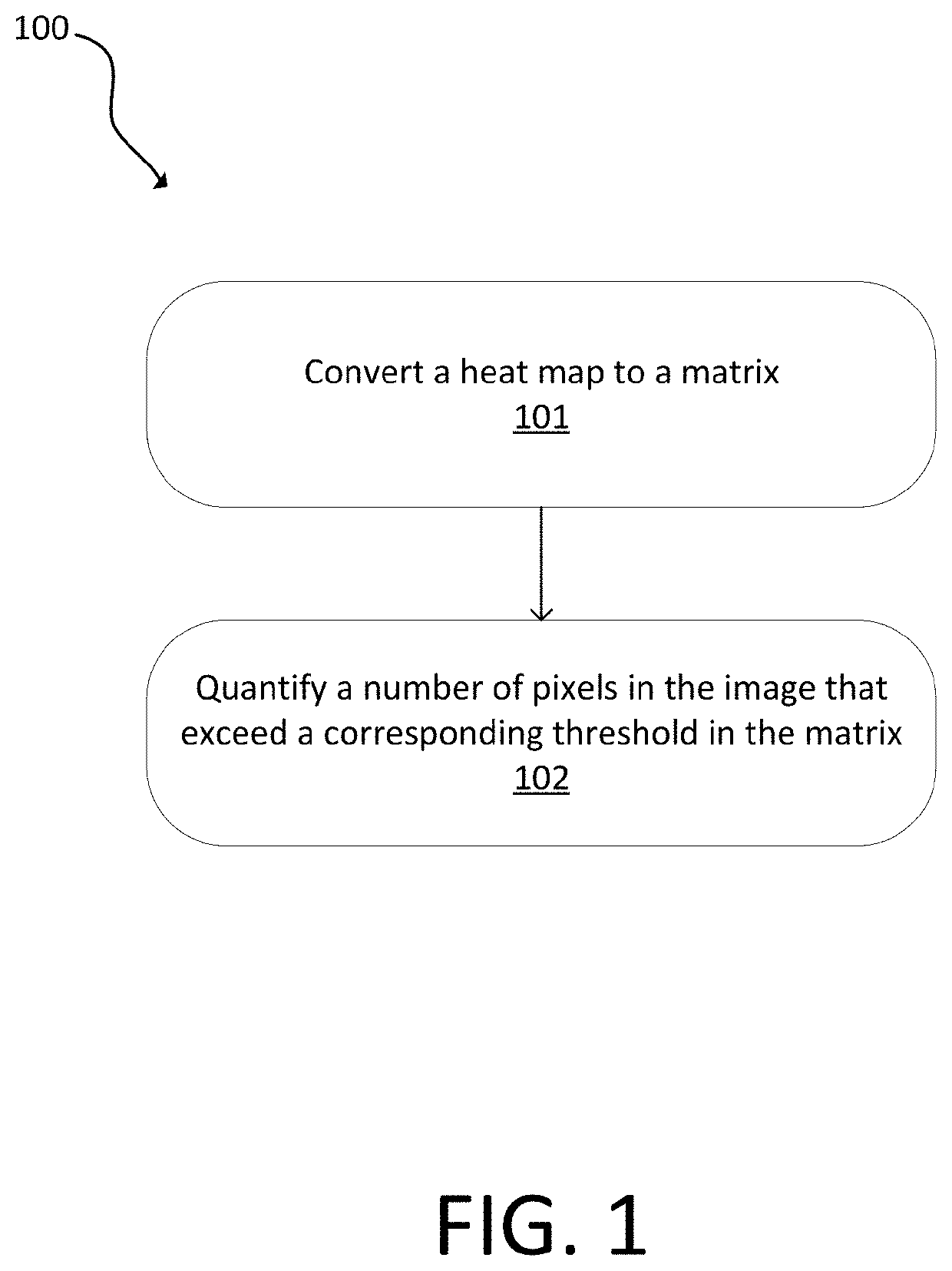
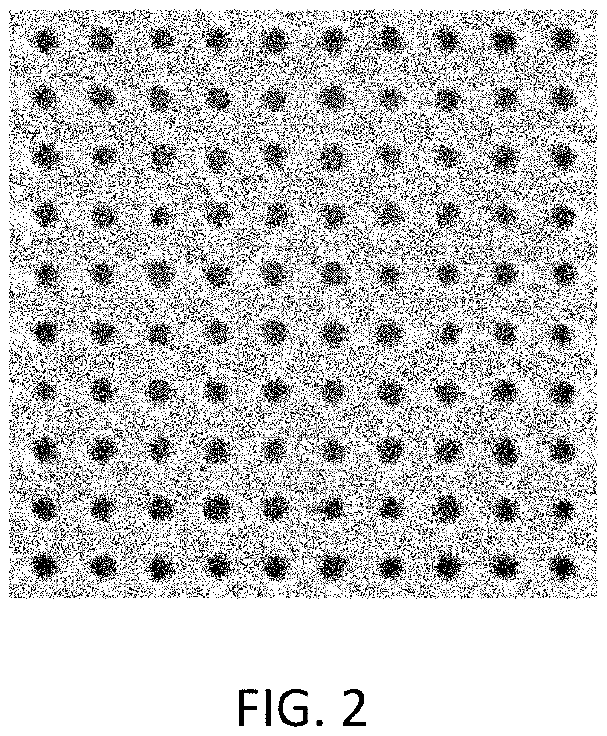
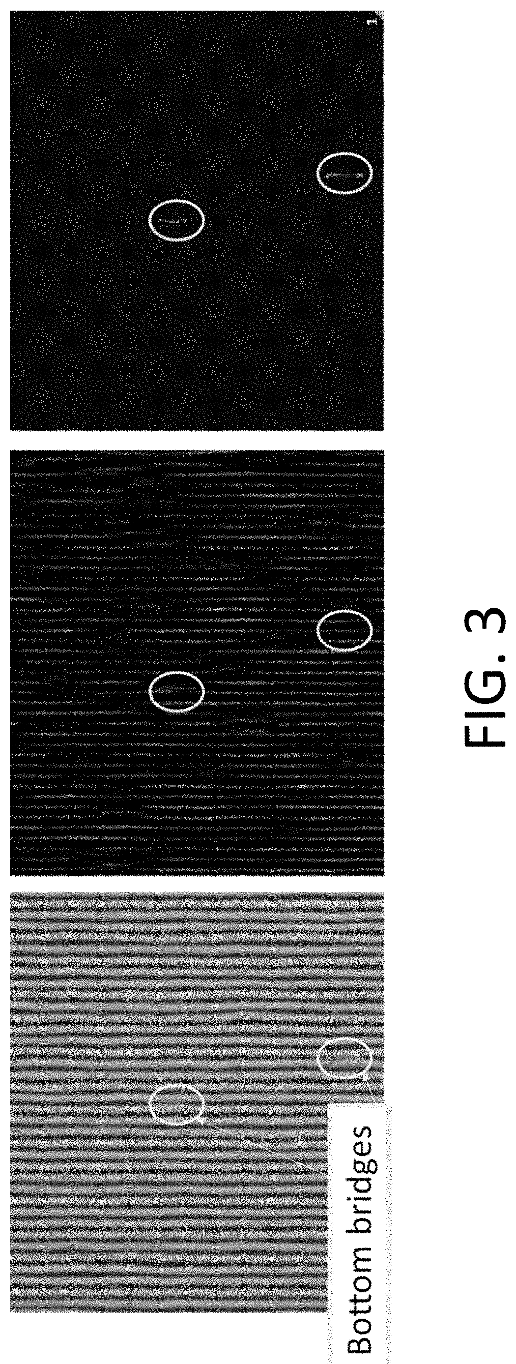
[0043]Embodiments disclosed herein use deep learning-based defect detection and / or classification networks for pixel level image quantification. For example, deep learning can be used for pixel level quantification of SEM images. This can be used in applications like extreme ultraviolet (EUV) stochastics rate quantification or critical dimension (CD) measurements / comparison. Embodiments disclosed herein can be integrated in the existing defect detection or classification schemes for review tools or inspection tools.

[0044]...


PUM


Abstract

A heat map of probable defects in an image can be represented as a matrix of defect probability index corresponding to each pixel. The image may be generated from data received from a detector of a scanning electron microscope or other inspection tools. A number of pixels in the image that exceed a corresponding threshold in the matrix can be quantified.

Description

CROSS-REFERENCE TO RELATED APPLICATIONS[0001]This application claims priority to the Indian patent application filed Nov. 15, 2018 and assigned App. No. 201841042919, the disclosure of which is hereby incorporated by reference.FIELD OF THE DISCLOSURE[0002]This disclosure relates to defect detection and classification.BACKGROUND OF THE DISCLOSURE[0003]Evolution of the semiconductor manufacturing industry is placing greater demands on yield management and, in particular, on metrology and inspection systems. Critical dimensions continue to shrink, yet the industry needs to decrease time for achieving high-yield, high-value production. Minimizing the total time from detecting a yield problem to fixing it determines the return-on-investment for a semiconductor manufacturer.[0004]Fabricating semiconductor devices, such as logic and memory devices, typically includes processing a semiconductor wafer using a large number of fabrication processes to form various features and multiple levels ...

Claims


Application Information

Patent Timeline
Patent Type & Authority Applications(United States)
IPC IPC(8): H01J37/22H01J37/28G06T7/00
CPCG06T7/0004H01J2237/2809G06T2207/10061G06T2207/20081G06T2207/30148H01J2237/2448H01J37/222H01J2237/2806H01J37/28H01J2237/2817H01J2237/221G06T2207/20084G01N21/9505G06T7/11
Inventor PATHANGI, HARIMEENAKSHISUNDARAM, SIVAPRRASATHBANSAL, TANAY
Owner KLA CORP
Why Eureka
Try Eureka