Thin-Film Transistor and Display Panel

a thin-film transistor and display panel technology, applied in the field of thin-film transistors and display panels, can solve the problems of difficult to increase the aperture ratio of subpixels and great difficulty in realizing high-resolution display devices, and achieve the effects of improving the output characteristics of thin-film transistors, improving the reliability of high-resolution display devices, and increasing the aperture ratio (or transmittance) of display panels

Active Publication Date: 2020-06-18
LG DISPLAY CO LTD
View PDF0 Cites 0 Cited by
  • Summary
  • Abstract
  • Description
  • Claims
  • Application Information

AI Technical Summary

Benefits of technology

[0014]According to exemplary embodiments, the output characteristics of the thin-film transistor can be improved by separating the top gate electrode (or bottom gate electrode) of the dual gate electrode into two electrodes and applying a back bias voltage to the top gate

Problems solved by technology

In existing display panels, there may be a problem that it is difficult to increase the aperture ratio of a subpixel using a c

Method used


Image

  • Thin-Film Transistor and Display Panel
  • Thin-Film Transistor and Display Panel
  • Thin-Film Transistor and Display Panel

Examples


Embodiment Construction

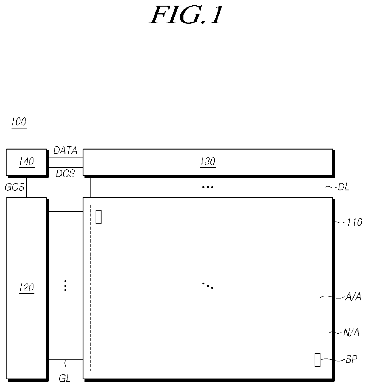
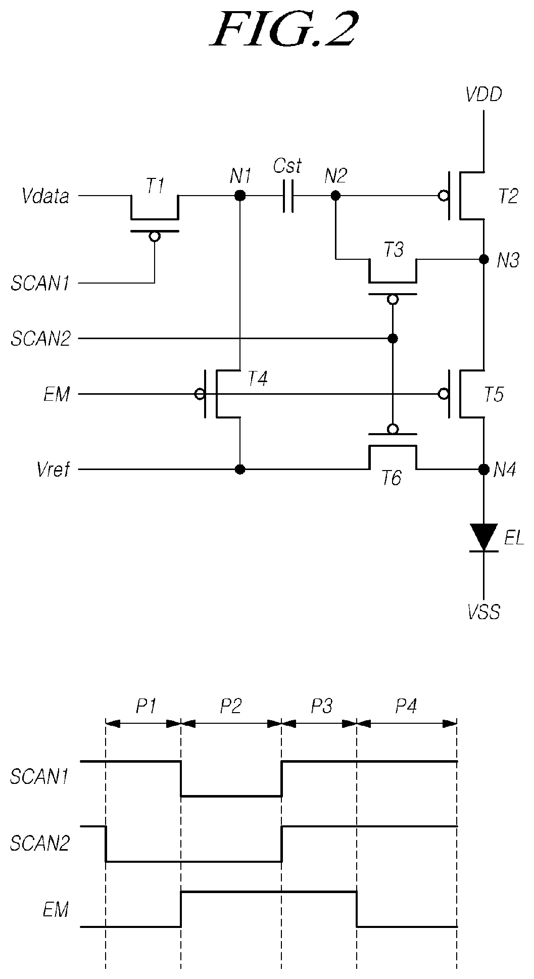
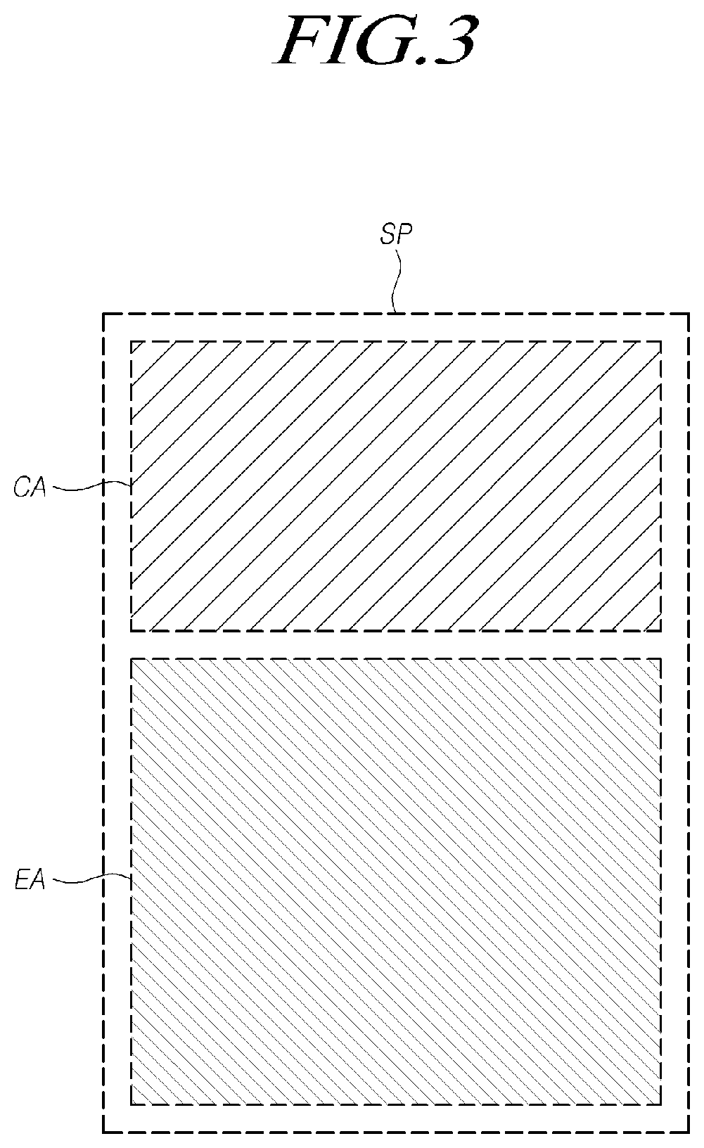
[0025]Hereinafter, reference will be made to exemplary embodiments in detail, examples of which are illustrated in the accompanying drawings. Throughout this document, reference should be made to the drawings, in which the same reference numerals and symbols will be used to designate the same or like components. In the following description of the present disclosure, detailed descriptions of known functions and components incorporated into the present disclosure will be omitted in the case that the subject matter of the present disclosure may be rendered unclear thereby.

[0026]It will also be understood that, while terms, such as “first,”“second,”“A,”“B,”“(a),” and “(b),” may be used herein to describe various elements, such terms are merely used to distinguish one element from other elements. The substance, sequence, order, or number of such elements is not limited by these terms. It will be understood that when an element is referred to as being “connected,”“coupled,” or “linked” t...


PUM


Abstract

A thin-film transistor and a display panel are provided in which current characteristics of the thin-film transistor are improved by a dual gate electrode structure, and the output characteristics of the thin-film transistor are improved by dividing the top gate electrode (or bottom gate electrode) of the dual gate electrode into two electrodes and applying a back bias voltage to the top gate electrode adjacent to a source region. A high-resolution display panel or a transparent display panel is realized by increasing the aperture ratio (or transmittance) of the display panel using the highly integrated high-current device.

Description

CROSS REFERENCE TO RELATED APPLICATION[0001]This application claims priority to Korean Patent Application No. 10-2018-0163871, filed on Dec. 18, 2018, which is hereby incorporated by reference for all purposes as if fully set forth herein.BACKGROUNDField[0002]Exemplary embodiments relate to a thin-film transistor and a display panel.Description of Related Art[0003]In response to the development of the information society, demand for a variety of types of display devices for displaying images is increasing. In this regard, a range of display devices, such as liquid crystal display (LCD) devices, and organic light-emitting diode (OLED) display devices, have come into widespread use.[0004]Such a display device includes, for example, a display panel in which a plurality of subpixels are disposed in the form of a matrix. The display device can display images by controlling luminous levels represented by the plurality of subpixels. In addition, a light-emitting element and a circuit eleme...

Claims


Application Information

Patent Timeline
IPC IPC(8): H01L29/786H01L29/10H01L29/78H01L27/12H01L29/423
CPCH01L29/7833H01L27/1214H01L29/78648H01L29/42356H01L29/1033H01L27/124H01L27/1248G09G3/3233G09G2300/0819G09G2300/0861G09G2300/0842G09G2300/0417G09G2320/0233H01L29/78696H01L29/78645G09G3/3208H01L29/78618H01L29/78606H10K59/1213
Inventor KO, SUNWOOKOH, KUMMI
Owner LG DISPLAY CO LTD
Why Eureka
Try Eureka