

Method for manufacturing conductive polymer thin film having semiconductor characteristic and thin-film transistor comprising conductive polymer thin film having semiconductor characteristic
a technology of conductive polymer and semiconductor properties, applied in the direction of conductive materials, solid-state devices, conductors, etc., can solve the problems of light loss in light alignment process, insufficient approach in minimizing light loss, and more severe light loss, so as to reduce light loss
- Summary
- Abstract
- Description
- Claims
- Application Information
AI Technical Summary
Benefits of technology
Problems solved by technology
Method used
Image

Examples
Embodiment Construction
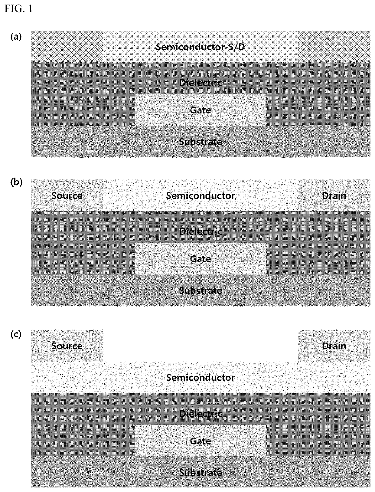
[0024]Hereinafter, embodiments of the present disclosure will be described in detail with reference to the accompanying drawings. The present disclosure may have various changes and may have various forms. Specific embodiments are illustrated in the drawings and described in detail therein. However, those embodiments are not intended to limit the present disclosure to any particular form thereof. It should be understood to include all changes, equivalents, or substitutes included in a spirit and scope in accordance with the present disclosure. In describing the drawings, similar reference numerals refer to similar components.
[0025]The terminology used herein is for the purpose of describing particular embodiments only and is not intended to be limiting the present disclosure. As used herein, the singular forms “a” and “an” are intended to include the plural forms as well, unless the context clearly indicates otherwise. It will be further understood that the terms “comprises”, “compr...
PUM
| Property | Measurement | Unit |
|---|---|---|
| temperature | aaaaa | aaaaa |
| temperature | aaaaa | aaaaa |
| current | aaaaa | aaaaa |
Abstract
Description
Claims
Application Information