Electronic Device Including a HEMT Including a Buried Region
a technology of buried regions and electronic devices, applied in semiconductor devices, diodes, electrical apparatus, etc., can solve problems such as high hysteresis, threshold voltage instability, and damage to plasmas
Inactive Publication Date: 2020-07-09
SEMICON COMPONENTS IND LLC
View PDF3 Cites 4 Cited by
- Summary
- Abstract
- Description
- Claims
- Application Information
AI Technical Summary
Benefits of technology
The patent text describes a new design for high-speed transistors. In one embodiment, a thicker portion of a region called the source-side buried is added to improve the performance of the transistor. This thicker portion helps with the dual depletion of the channel and increases the electron density. In another embodiment, a dielectric layer is used in the gate structure, which can cause plasma damage and generate interface states or traps that affect the performance of the transistor. The text aims to improve the performance of enhancement-mode high electron mobility transistors without the adverse complications caused by the dielectric layer.
Problems solved by technology
A barrier layer can be etched and cause plasma damage that generates interface states or traps between the etched (plasma damaged) semiconductor surface and a subsequently-deposited gate dielectric.
This can cause high hysteresis, threshold voltage instability, and relatively higher gate leakage and relatively lower gate voltage overdrive as compared to a depletion-mode high electronic mobility transistor.
Method used
View moreImage
Smart ImageViewing Examples

Examples
embodiment 1
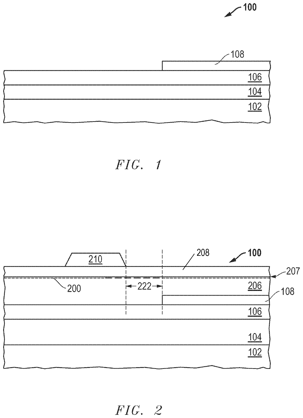
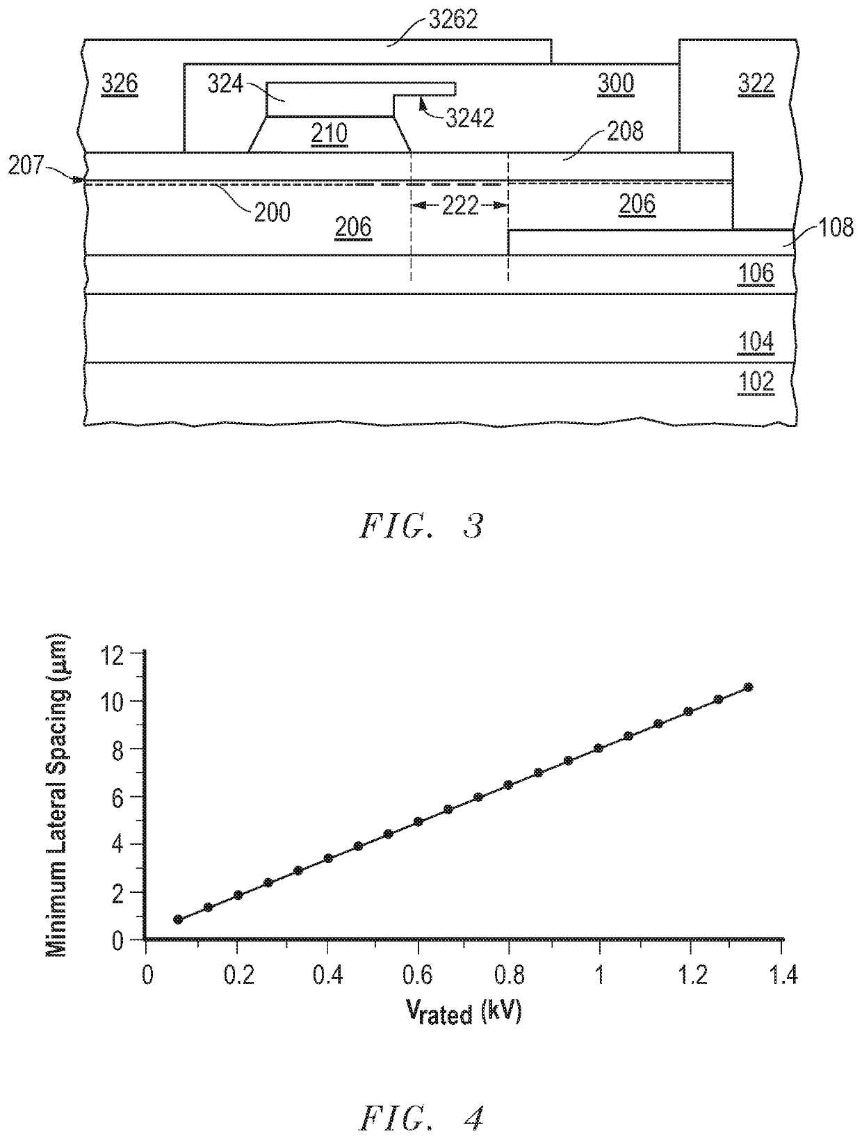
[0073]An electronic device can include a high electron mobility transistor including a first buried region; a channel layer overlying the first buried region; a gate electrode; and a drain electrode overlying the first buried region. The first buried region can extend toward and does not underlie the gate electrode.
embodiment 2
[0074]The electronic device of Embodiment 1, wherein the first buried region includes a p-type semiconductor material.
embodiment 3
[0075]The electronic device of Embodiment 2, wherein the channel layer and the first buried region have a same base semiconductor material.
Login to View More PUM
| Property | Measurement | Unit |
|---|---|---|
| thickness | aaaaa | aaaaa |
| thickness | aaaaa | aaaaa |
| rated voltage | aaaaa | aaaaa |
Abstract
An electronic device can include a high electron mobility transistor that includes a buried region, a channel layer overlying the buried region, a gate electrode, and a drain electrode overlying the buried region. The buried region can extend toward and does not underlie the gate electrode. In a particular aspect, the electronic device can further include a p-type semiconductor member overlying the channel layer. The gate electrode can overlie the channel layer, a p-type semiconductor member overlying the channel layer. The drain electrode can overlie and contact the buried region and the p-type semiconductor member. The p-type semiconductor member can be disposed between the gate and drain electrodes. In another embodiment, a source-side buried region may be used in addition to or in place of the buried region that is coupled to the drain electrode.
Description
FIELD OF THE DISCLOSURE[0001]The present disclosure relates to electronic devices, and more particularly to, electronic devices including high electron mobility transistors including buried regions.RELATED ART[0002]High electron mobility transistors can be enhancement-mode transistors. One type of such transistor can include a p-type GaN gate structure. In one configuration, a barrier layer is etched and the p-type GaN is formed within the opening. Transistors with p-type GaN gate structures typically have higher dynamic on-state resistance due to plasma-induced damage from a pGaN etch in access regions. The transistor can also have relatively high on-state gate leakage as compared to depletion-mode high electron mobility transistors. When the p-type GaN includes Mg, some Mg may diffuse into the GaN channel layer and increase on-state resistance.[0003]Alternatively, an enhancement-mode transistor can be formed with a dielectric layer as part of the gate structure. A barrier layer ca...
Claims
Login to View More Application Information
Patent Timeline
 Patent Type & Authority Applications(United States)
IPC IPC(8): H01L27/06H01L29/20H01L29/205H01L29/40H01L29/778
CPCH01L29/2003H01L27/0629H01L29/7787H01L29/402H01L29/0623H01L29/7786H01L21/8252H01L27/0605H01L27/0727H01L29/0619H01L29/0688H01L29/404H01L29/41766
Inventor MOENS, PETERSTOCKMAN, ARNOVANMEERBEEK, PIETBANERJEE, ABHISHEKDECLERCQ, FREDERICK JOHAN G.
Owner SEMICON COMPONENTS IND LLC