Smart interface circuit

a technology of interface circuit and intelligent interface, applied in the field of interface circuit, can solve the problems of wasting pcie transmission bandwidth, and achieve the effect of reducing transmission bandwidth waste and accelerating data reading operation

Active Publication Date: 2020-07-30
REALTEK SEMICON CORP
View PDF0 Cites 1 Cited by
  • Summary
  • Abstract
  • Description
  • Claims
  • Application Information

AI Technical Summary

Benefits of technology

The patent is about a new interface circuit that improves data reading to save transmission bandwidth. The circuit helps to speed up data reading, making it faster and more efficient.

Problems solved by technology

Since the transmission speed of a PCIe interface is higher than the transmission speed of a USB interface, at the moment the NVMe storage device finishes outputting the first data to the NVMe host, normally the USB device has not finished outputting the first data to the USB host yet; therefore, the NVMe host has to wait for a while before transmitting the second doorbell signal to the NVMe storage device, which wastes the PCIe transmission bandwidth.

Method used


Image

  • Smart interface circuit
  • Smart interface circuit
  • Smart interface circuit

Examples


Embodiment Construction

[0027]The smart interface circuit of the present disclosure can accelerate data access operation in comparison with the prior art, and thereby reduce the waste of transmission bandwidth.

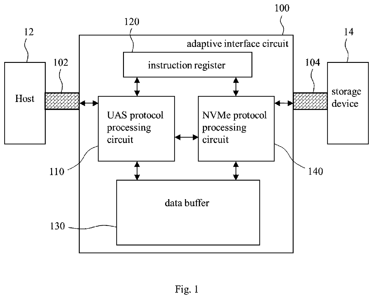
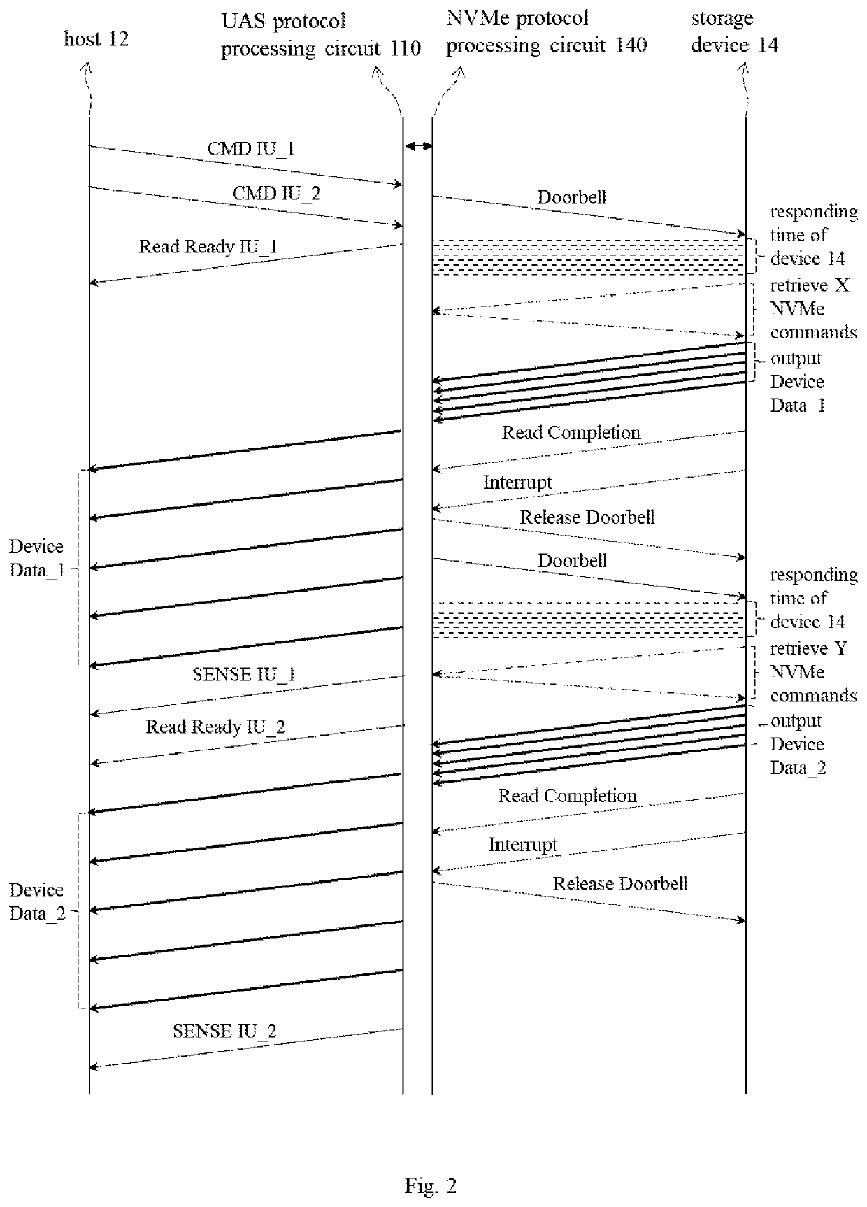
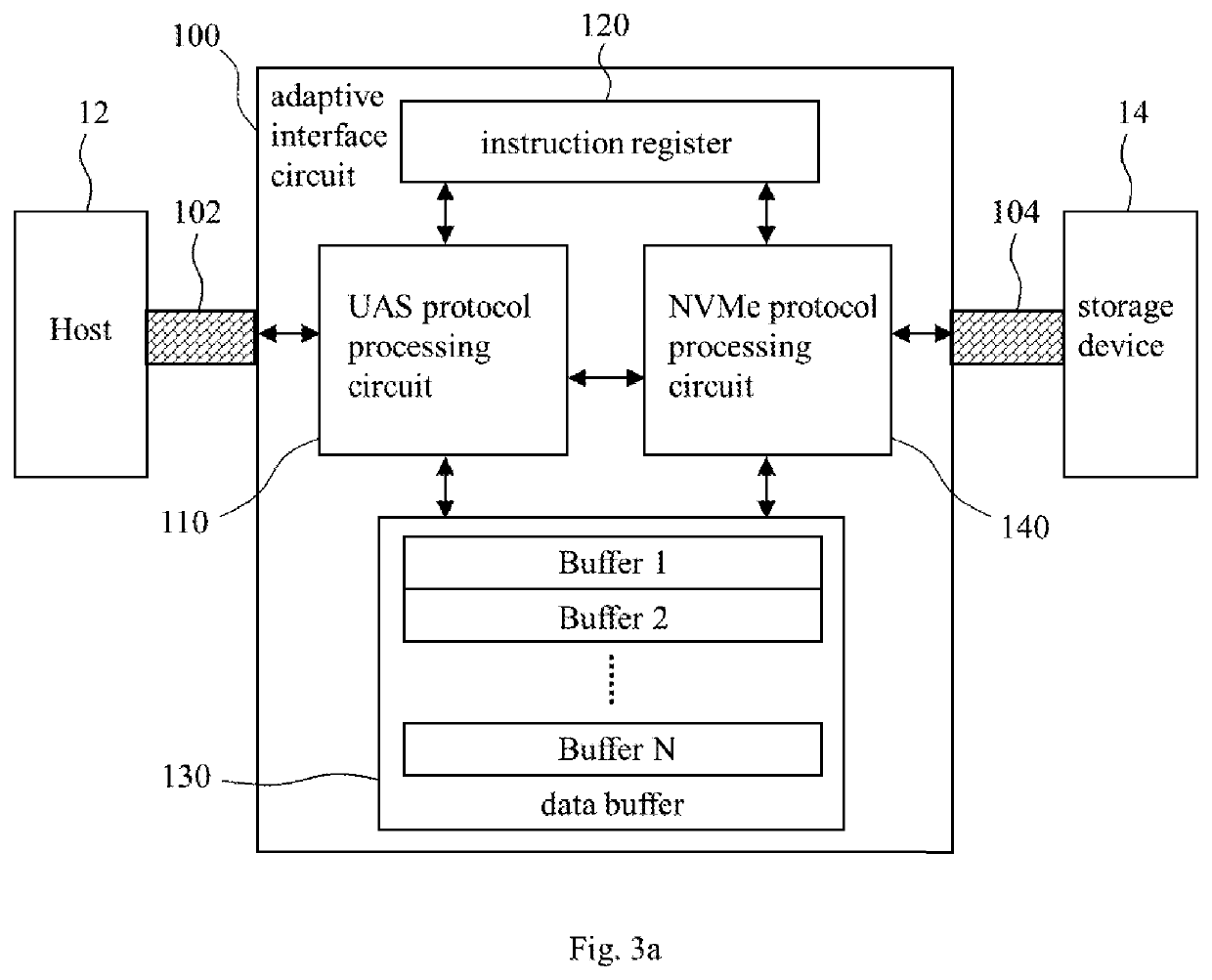
[0028]FIG. 1 shows an embodiment of the smart interface circuit of the present disclosure; and FIG. 2 illustrates the communication procedures of the smart interface circuit 100 of FIG. 1, wherein the vertical direction of FIG. 2 can be deemed the direction of a time axis. The smart interface circuit 100 is configured to couple a first interface 102 with a second interface 104, and includes a first protocol processing circuit 110 (e.g., a UAS (USB Attached SCSI) protocol processing circuit), an instruction register 120, a data buffer 130, and a second protocol processing circuit 140 (e.g., an NVMe (Non-Volatile Memory Express) protocol processing circuit).

[0029]Please refer to FIGS. 1-2. The first protocol processing circuit 110 is configured to output data to a first device 12 (e.g., a host such as ...


PUM


Abstract

A smart interface circuit includes: a first protocol processing circuit receiving several first protocol commands including a first command and a second command from a first device, storing the commands in an instruction register that is accessible to a second protocol processing circuit, and outputting first data and second data stored in a data buffer to the first device according to the first command and the second command respectively; and the second protocol processing circuit generating X second protocol command(s) according to the first command to request a second device to output the first data to the data buffer, and before the first protocol processing circuit finishes outputting the first data to the first device, the second protocol processing circuit generating Y second protocol command(s) according to the second command to request the second device to output the second data to the data buffer.

Description

BACKGROUND OF THE INVENTION1. Field of the Invention[0001]The present invention relates to an interface circuit, especially to a smart interface circuit.2. Description of Related Art[0002]The USB (Universal Serial Bus) to PCIe (Peripheral Component Interconnect Express) adapter technique follows the UAS (USB Attached SCSI (Small Computer System Interface)) protocol and NVMe (Non-Volatile Memory Express) protocol. The two protocols are described in brief below.[0003](1) UAS protocol: This protocol specifies the way to exchange data between a USB host (e.g., a personal computer) and a USB device (i.e., a USB-to-PCIe adapter functioning as a USB device here), the way including:[0004](i) the USB host (a.k.a. a UAS initiator port) transmitting a COMMAND IU (Command Information Unit) to the USB device;[0005](ii) after the USB device (a.k.a. a UAS target port) is available to execute instructions, the USB device replying to the USB host with a WRITE / READ READY IU and then the both sides st...

Claims


Application Information

Patent Timeline
Patent Type & Authority Applications(United States)
IPC IPC(8): G06F13/42G06F13/16
CPCG06F2213/0026G06F2213/0042G06F13/4221G06F13/4282G06F2213/28G06F13/1684G06F13/4068G06F13/4022G06F13/387
Inventor LIN, CHIA-HUNGTSENG, MIN-YU
Owner REALTEK SEMICON CORP
Why Eureka
Try Eureka