Magnetic thin-film memory device for quick and stable reading data
- Summary
- Abstract
- Description
- Claims
- Application Information
AI Technical Summary
Benefits of technology
Problems solved by technology
Method used
Image

Examples
first embodiment
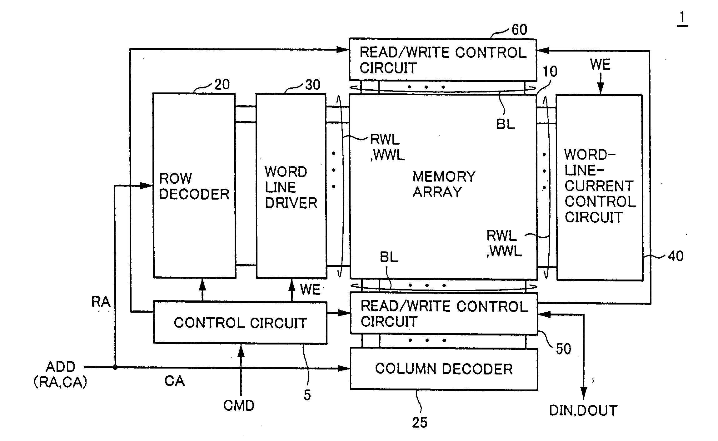
[0108] Referring to FIG. 1, an MRAM device 1 of the first embodiment of the present invention performs random access in response to a control signal CMD and an address signal ADD supplied from an external unit to input write data DIN and output read data OUT.
[0109] The MRAM device 1 is provided with a control circuit 5 for controlling all operations of the MRAM device 1 in response to the control signal CMD and a memory array 10 having a plurality of MTJ memory cells arranged in a matrix (n rows×m columns). Though the configuration of the memory array 10 will be described later in detail, a plurality of write word lines WWL and a plurality of read word lines RWL are arranged correspondingly to rows of MTJ memory cells and a plurality of bit lines BL are arranged correspondingly to columns of the MTJ memory cells.
[0110] The MRAM device 1 is further provided with a row decoder 20 for executing row selection in the memory array 10 correspondingly to a row address RA shown by an addre...
second embodiment
[0157] Referring to FIG. 10, in the case of a memory array 10 according to the second embodiment, read word lines RWL are hierarchically arranged with main read word lines MRWL. The read word lines RWL are arranged every memory cell row independently of regions AR1 and AR2 similarly to the case of the first embodiment. Therefore, read word lines RWL11 to RWL1n and RWL21 to RWL2n are arranged on the whole of a memory array 10. Subdrivers RSD11 to RSD1n and RSD21 to RWD2n correspond to read word lines.
[0158] The main read word line MRWL is provided along the column direction in common to the regions AR1 and AR2. The main word line MRWL is provided every L (L: natural number) memory cell rows. Thereby, each read word line RWL is related with any one of main read word lines MRWL1 to MRWLj (j=natural number shown by n / L).
[0159]FIG. 9 shows a case of L=4 as an example, that is, a configuration in which one main read word line MRWL is arranged every four memory cell rows. Thus, by arrang...
third embodiment
[0168] Referring to FIG. 14, in the memory array 10 of the third embodiment, a read word line and a write word line are respectively constituted of a common word line RWWL. That is, in the case of the memory array 10 of the third embodiment, word lines RWWL1 to RWWLn are arranged for each memory cell row and the word line RWWL is used for data read and data write in common. A word-line-current control circuit 40 has current control transistors 41-1 to 41-n corresponding to the word lines RWWL1 to RWWLn.
[0169] Referring to FIG. 15, a word line RWWL is constituted as a metallic wiring on the same layer as the gate 130 of an access transistor ART made of a low-resistance material. The low-resistance material for constituting the gate of the access transistor ATR can use a metal such as tungsten. Thereby, it is possible to omit a metallic wiring layer (metallic wiring layer M2 in FIG. 27) on which write word lines WWL have been arrange so far, compared to the structure of a conventiona...
PUM
 Abstract
Description
Claims
Application Information
 - R&D Engineer
- R&D Manager
- IP Professional
- Industry Leading Data Capabilities
- Powerful AI technology
- Patent DNA Extraction
Browse by: Latest US Patents, China's latest patents, Technical Efficacy Thesaurus, Application Domain, Technology Topic.
© 2024 PatSnap. All rights reserved.Legal|Privacy policy|Modern Slavery Act Transparency Statement|Sitemap