

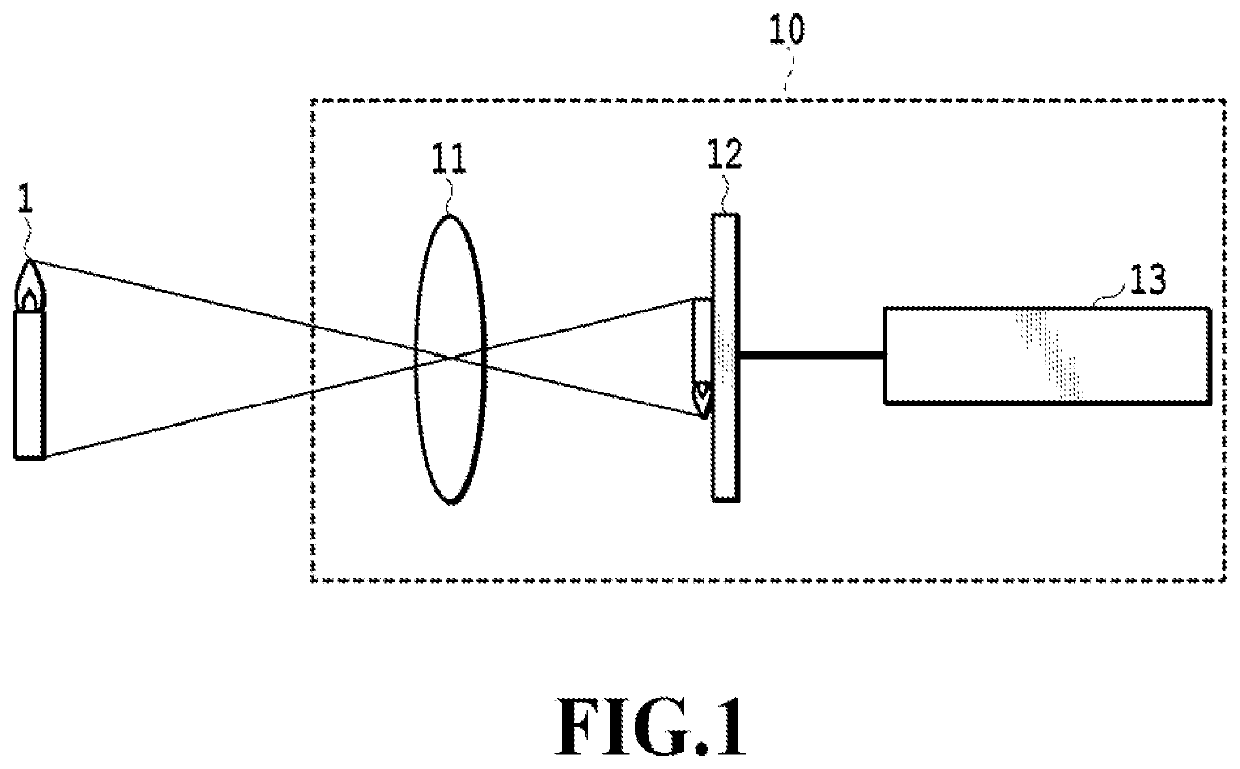
Color image-capture element and image capture device
a technology of image capture and element, applied in the direction of optical filter, semiconductor device, radio frequency control device, etc., can solve the problems of not being able to achieve photoelectric conversion, remaining lost light constitutes loss due to absorption or reflection, and becomes about 13, and achieves low polarization dependence, simple manufacturing, and high light utilization ratio
- Summary
- Abstract
- Description
- Claims
- Application Information
AI Technical Summary
Benefits of technology
Problems solved by technology
Method used
Image

Examples
embodiment 1
[0077]Hereinafter, an outline of a configuration of an image capture element according to Embodiment 1 will be described
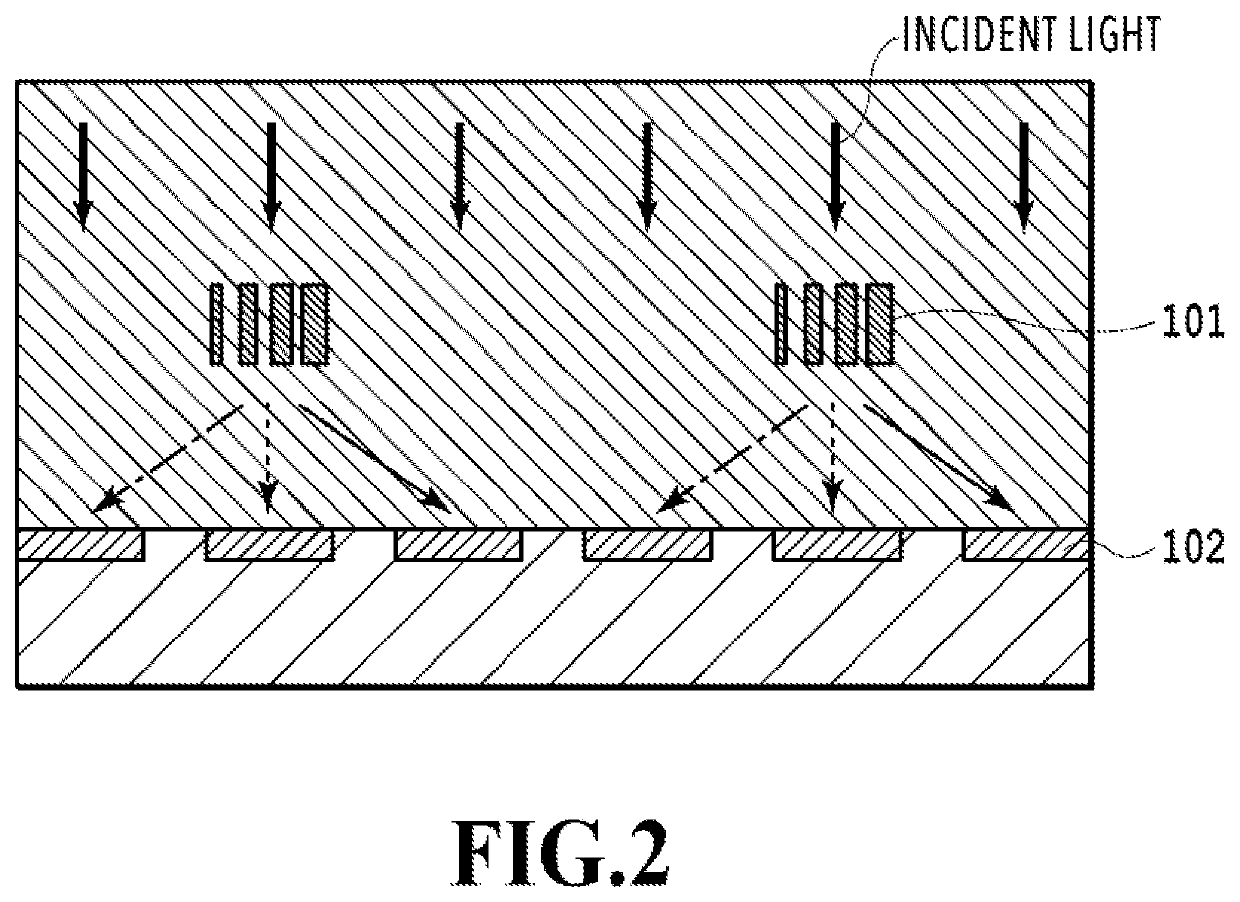
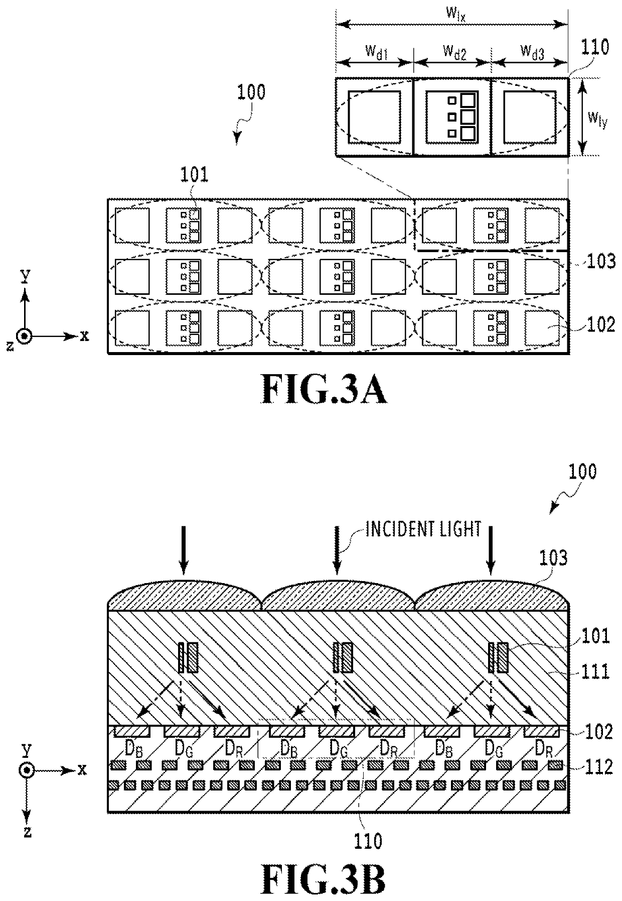
[0078]FIG. 3A is a top view of a schematic configuration of a part of the image capture element according to Embodiment 1 of the present invention, and FIG. 3B is a sectional view thereof. An image capture element 100 according to Embodiment 1 has a transparent layer 111 having a low refractive index made of SiO2 or the like and a plurality of micro-lenses 103 laminated on a two-dimensional pixel array in which pixels 102 each including a photoelectric conversion element are disposed in an array. Inside the transparent layer 111 having the low refractive index, micro-spectroscopic elements 101 each including a plurality of microstructures having constant thickness (length in a direction perpendicular to the two-dimensional pixel array) formed of a material such as SiN having a higher refractive index than that of the transparent layer 111 are embedded. For the sake...
embodiment 2
[0117]Next, an image capture element according to Embodiment 2 of the present invention will be described.
[0118]FIG. 12A is a top view of a schematic configuration of a part of the image capture element according to Embodiment 2 of the present invention, and FIG. 12B is a sectional view thereof. As shown in FIGS. 12A and 12B, an image capture element 300 of Embodiment 2 and an image capture device using it is different from Embodiment 1 in that the direction of a structure pattern of a plurality of micro-spectroscopic element 101 disposed along the x-axis direction is alternately reversed.
[0119]The rows of the micro-spectroscopic elements 101 and color pixel units U formed along the x-axis direction are sequentially disposed in the y-axis direction while shifting in the x-axis direction by a two-pixel size, and as a result, the direction of the structure pattern of the micro-spectroscopic element 110 is alternately reversed in the y-axis direction also. Furthermore, there is also di...
embodiment 3
[0125]Next, an image capture element according to Embodiment 3 of the present invention will be described.
[0126]FIG. 14A is a top view of a schematic configuration of a part of the image capture element according to Embodiment 3 of the present invention, and FIG. 14B is a sectional view thereof. As shown in FIGS. 14A and 14B, an image capture element 400 of Embodiment 3 and an image capture device are different from Embodiment 1 in that micro-lenses are disposed so as to correspond to the respective pixels on a one-on-one basis. In addition, they are also different in that matrix calculation using the photoelectric conversion signal from each pixel 102 is used for obtaining color information. Other components are the same as those in Embodiment 1. The description below will focus on differences from Embodiment 1 and description of overlapping points will be omitted.
[0127]As shown in FIG. 14B, micro-lenses 103 are disposed so as to correspond to the respective pixels 102 on a one-on-...
PUM
| Property | Measurement | Unit |
|---|---|---|
| blue wavelength | aaaaa | aaaaa |
| wavelength region | aaaaa | aaaaa |
| red wavelength | aaaaa | aaaaa |
Abstract
Description
Claims
Application Information