Electronic device

a technology of electronic devices and peripheral traces, applied in the field of electronic devices, can solve the problems of insufficient degree of reducing the border by conventional techniques, low reliability of such electronic devices manufactured by conventional techniques, etc., and achieve the effects of enhancing the yield of peripheral traces, reducing the border and size of electronic devices, and improving the quality of electronic devices

Inactive Publication Date: 2020-10-08
HANNSTAR DISPLAY NANJING +1
View PDF0 Cites 0 Cited by
  • Summary
  • Abstract
  • Description
  • Claims
  • Application Information

AI Technical Summary

Benefits of technology

[0004]The present invention provides an electronic device, wherein a peripheral region of a flexible substrate has a bending part and a cutting structure adjacent to the bending part, such that the peripheral region of the flexible substrate can be bended to reduce the border and downsized the electronic device under the condition that the reliability of the electronic device is not affected.
[0006]The peripheral region of the present invention is bended backward to the back of the active region to reduce the border and size of the electronic device by bending ways. Furthermore, the flexible substrate has the cutting structures in the peripheral region which can determine the extending lines and separate the bending parts, when the bending ways are proceeded on the peripheral region, at least one of the bending parts of the peripheral region may be bended according to the corresponding extending line, such that the main bending portions having the peripheral traces and / or the electronic components are only bended one time, so as to enhance the yield of the peripheral traces and further improve qualities of the electronic device.

Problems solved by technology

However, the reliability of such electronic device manufactured by the conventional techniques is low (for example, the trace of the electronic device may be broken to be an open circuit), or the degree of reducing the border by the conventional techniques is insufficient.

Method used


Image

  • Electronic device
  • Electronic device
  • Electronic device

Examples


Embodiment Construction

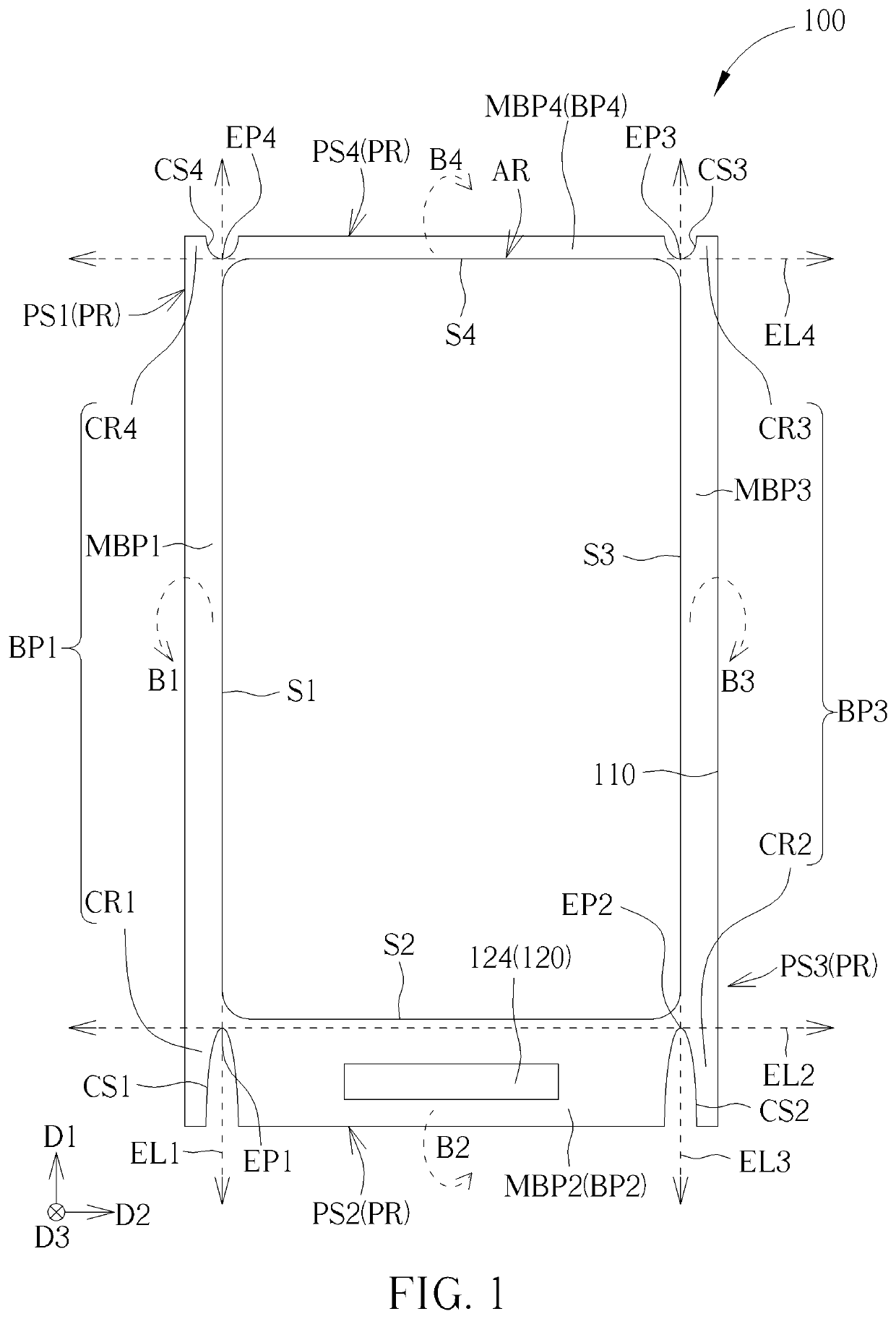
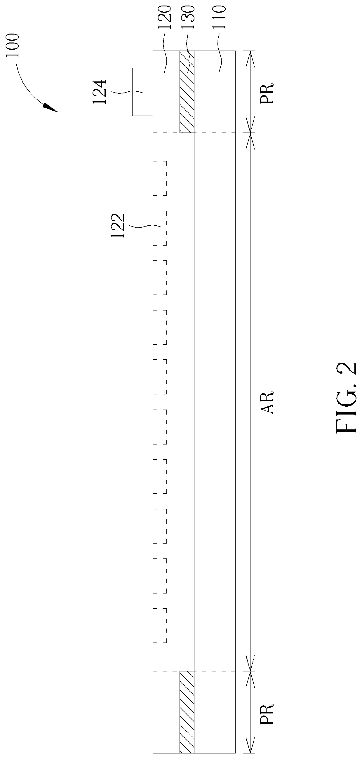
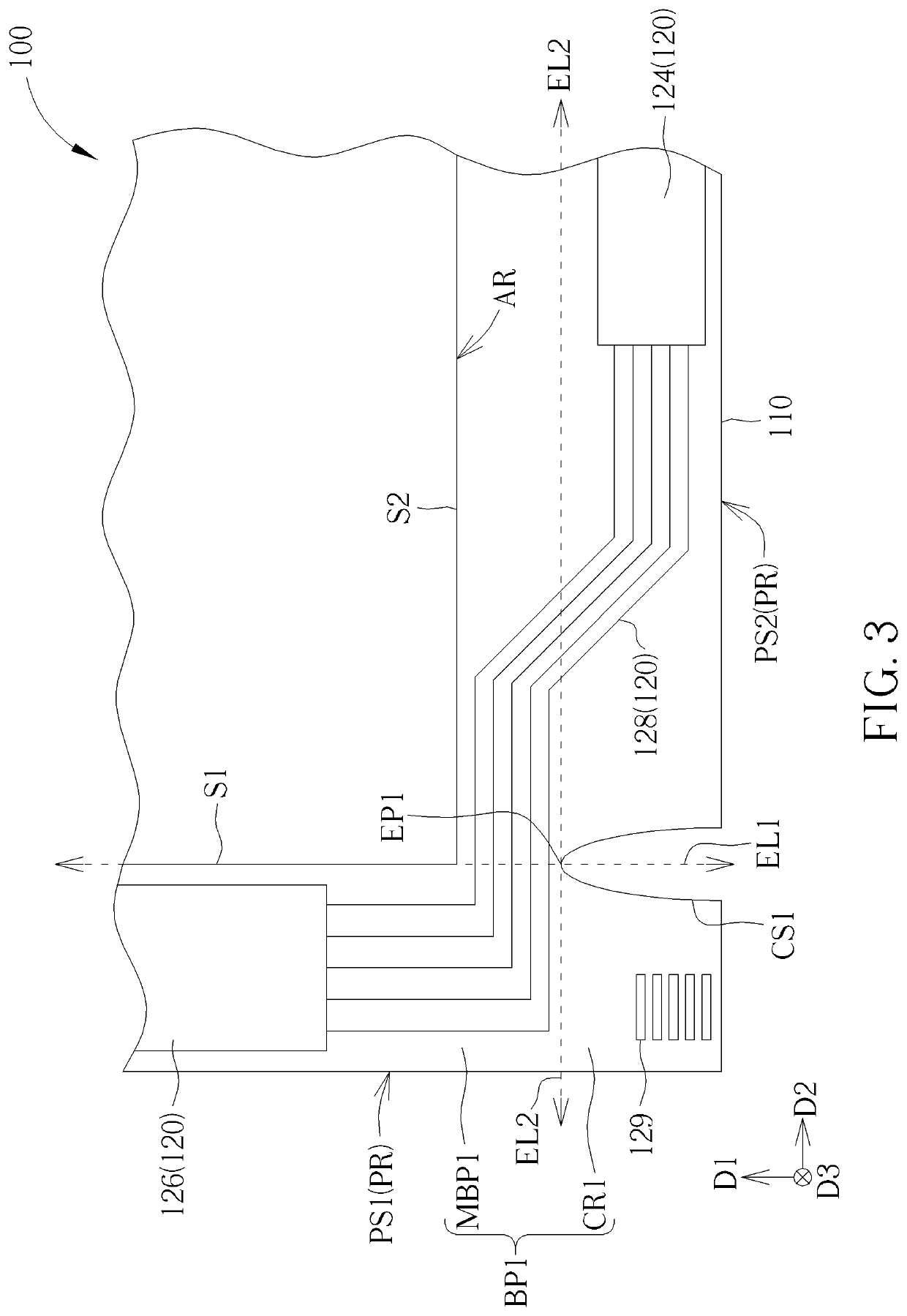
[0021]To provide a better understanding of the present invention to those skilled in the art, some embodiments will be detailed in the following description. The embodiments of the present invention are illustrated in the accompanying drawings with numbered elements to elaborate on the contents and effects to be achieved. It should be noted that the drawings are simplified schematics, and therefore show only the components and combinations associated with the present invention, so as to provide a clearer description for the basic structure or implementing method of the present invention. The components would be more complex in reality. In addition, for ease of explanation, the components shown in the drawings may not represent their actual number, shape, and dimensions; details may be adjusted according to design requirements.

[0022]Note that the terms “back”, “rear”, “backward” and “behind” described herein refer to the relative relationship in a top view direction. For instance, if...


PUM


Abstract

An electronic device includes a flexible substrate and a peripheral trace. The flexible substrate includes an active region and a peripheral region situated outside of the active region. The flexible substrate includes a first bending part, a second bending part and a first cutting structure in the peripheral region. The first bending part is disposed on a first side region of the peripheral region and extending along a first direction. The second bending part is disposed on a second side region of the peripheral region and extending along a second direction not parallel to the first direction, and the second side region is adjacent to the first side region. The first cutting structure is adjacent to the first bending part and the second bending part. The peripheral trace is disposed on the flexible substrate and disposed between the active region and the first cutting structure.

Description

CROSS REFERENCE TO RELATED APPLICATION[0001]This application claims the benefit of priority of China Application Serial No. 201910262389.X, which was filed on Apr. 2, 2019. The entirety of the above-mentioned patent application is hereby incorporated herein by reference and made a part of this specification.BACKGROUND OF THE INVENTION1. Field of the Invention[0002]The present invention relates to an electronic device, and more particularly to an electronic device having a bending part in a peripheral region.2. Description of the Prior Art[0003]Nowadays, electronic devices have become an indispensable item in society. For example, since the electronic device such as a display device or a touch display device has the characteristics of thin appearance, light weight, low power consumption and no radiation pollution, it has been widely used in many kinds of electronic products, such as notebooks, smart phones, watches, and display devices in vehicles, for transmitting and displaying inf...

Claims


Application Information

Patent Timeline
Patent Type & Authority Applications(United States)
IPC IPC(8): H01L27/12H01L23/552
CPCH01L23/552H01L27/124H01L27/1218G06F3/0412G06F3/0416
Inventor CHEN, YEN-CHUNG
Owner HANNSTAR DISPLAY NANJING
Why Eureka
Try Eureka