Wide gap semiconductor device
- Summary
- Abstract
- Description
- Claims
- Application Information
AI Technical Summary
Benefits of technology
Problems solved by technology
Method used
Image

Examples
first embodiment
>
[0042]In the present embodiment, description will be given using a vertical MOSFET as an example. In the present embodiment, a first conductivity type is described as an n-type, and a second conductivity type is described as a p-type. However, the present embodiment is not limited to such an aspect, and the first conductivity type may be the p-type, and the second conductivity type may be the n-type. Additionally, in the present embodiment, description will be given using silicon carbide as a wide gap semiconductor. However, the present embodiment is not limited to such an aspect, and gallium nitride or the like may be used as the wide gap semiconductor.
[0043]In the present embodiment, an in-plane direction including an X direction and a Y direction in FIG. 1 is referred to as a plane direction. A Z direction orthogonal to the X direction and the Y direction is a thickness direction of the semiconductor device, and is also referred to as an up-and-down direction.
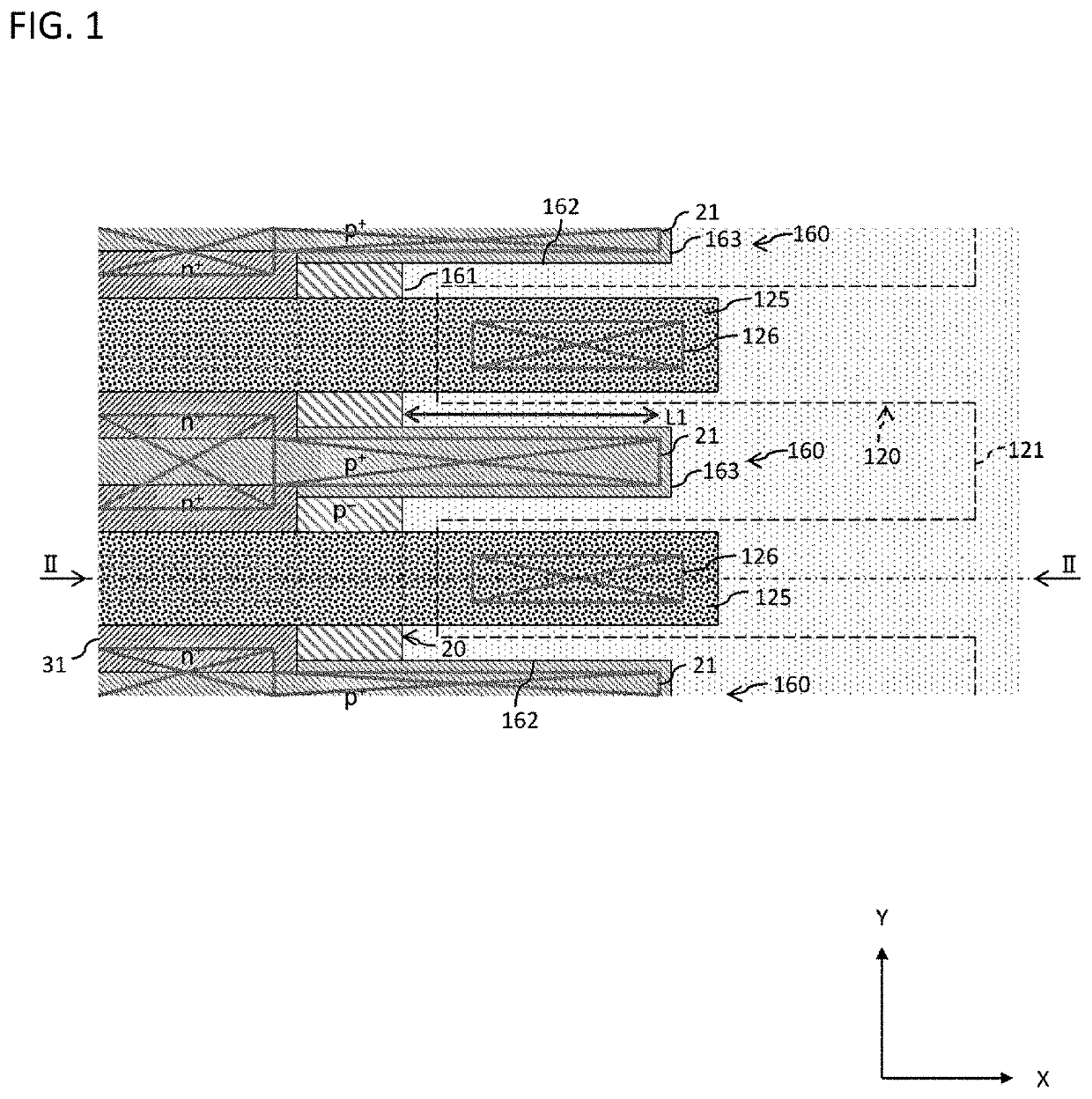
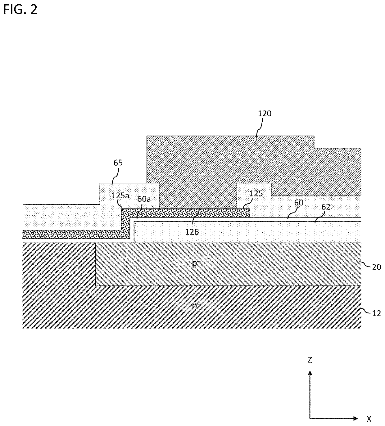
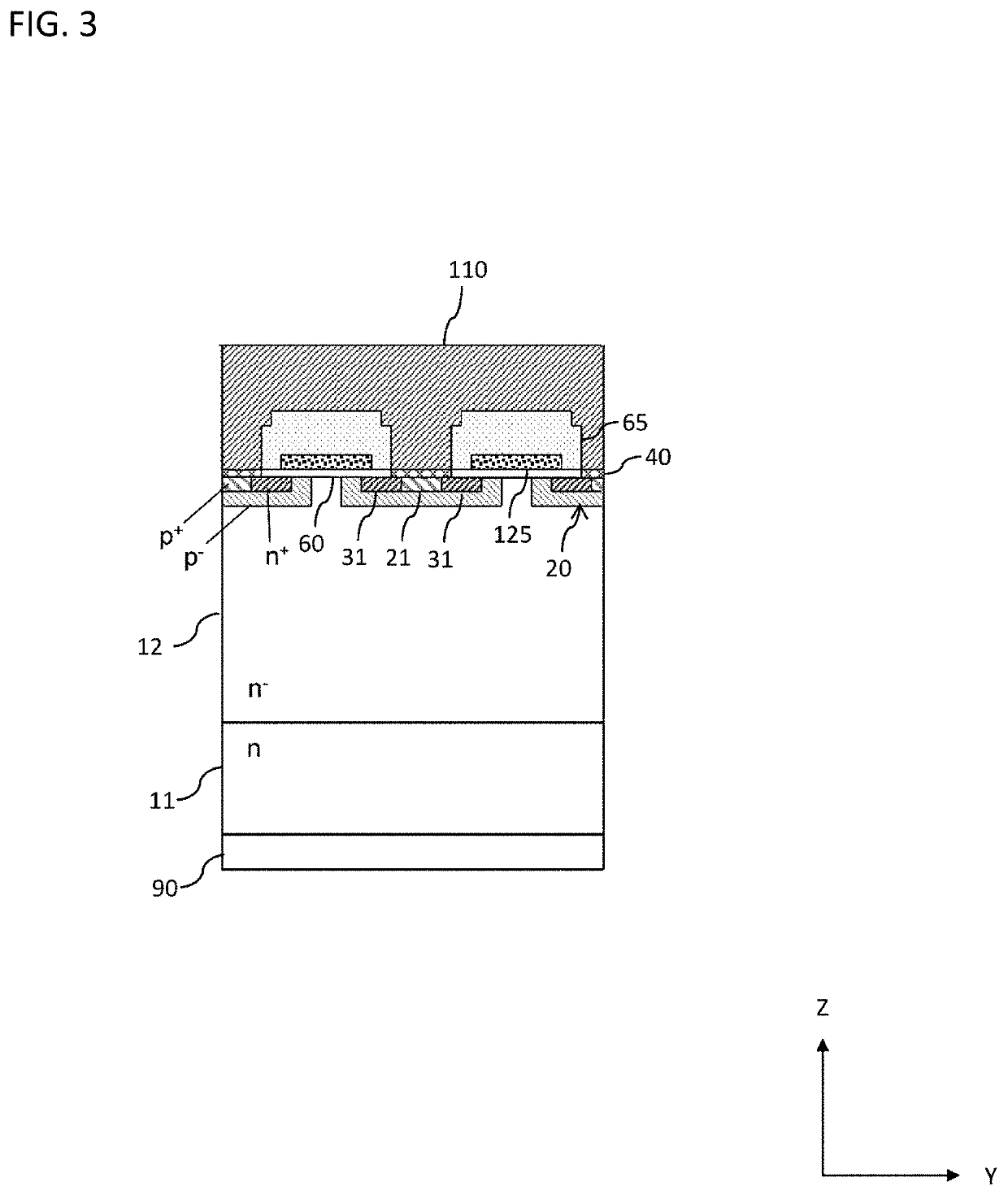
[0044]As shown in F...
second embodiment
[0063]Next, a second embodiment of the present invention will be described.
[0064]In the present embodiment, as shown in FIG. 4 and FIG. 5, a peripheral slit 15 reaching a drift layer 12 is provided in a well region 20 and in a side of a source region 31 than a gate contact hole (that is, closer to the side of the source region 31 than a gate connection region 126) in the plane direction. More specifically, the peripheral slit 15 has a first peripheral slit 15a extending along a Y direction while being connected to the drift layer 12 across the well region 20 provided below a field insulating film 62 (particularly see FIG. 5) and a second peripheral slit 15b provided at both ends of the first peripheral slit 15a and extending in an X direction while being connected to the drift layer 12 across the well region 20. Others are the same as those in the first embodiment, and any configuration adopted in the first embodiment can be adopted also in the second embodiment. Members described i...
third embodiment
[0068]Next, a third embodiment of the present invention will be described.
[0069]In the present embodiment, as shown in FIG. 6 and FIG. 7, a well contact region 21 extends to a side opposite to a source region 31 (the right side in FIG. 6) further than an end of a gate electrode 125 in the side opposite to the source region 31 (the left end of L2 shown by a double-headed arrow in FIG. 6). More specifically, the well contact region 21 extends to the right in an X direction further than the right end of the gate electrode 125 in the X direction in FIG. 6. Also in the present embodiment, any configuration adopted in each of the above embodiments can be adopted. Members described in the above embodiments will be described with the same reference numerals.
[0070]The adoption of an aspect like the present embodiment is advantageous in that even if resistance in the well contact region 21 is high, an increase in potential of a well region 20 of a p-type at a position below a gate insulating ...
PUM
 Abstract
Description
Claims
Application Information
 - R&D Engineer
- R&D Manager
- IP Professional
- Industry Leading Data Capabilities
- Powerful AI technology
- Patent DNA Extraction
Browse by: Latest US Patents, China's latest patents, Technical Efficacy Thesaurus, Application Domain, Technology Topic.
© 2024 PatSnap. All rights reserved.Legal|Privacy policy|Modern Slavery Act Transparency Statement|Sitemap