Display device and manufacturing method thereof

a technology of a display device and a manufacturing method, applied in the field of display devices, can solve the problems of reducing yield, increasing cost, and film requires a more complicated process, and achieve the effect of high reliability and high electric characteristics

Inactive Publication Date: 2010-09-07
SEMICON ENERGY LAB CO LTD
View PDF17 Cites 40 Cited by
  • Summary
  • Abstract
  • Description
  • Claims
  • Application Information

AI Technical Summary

Benefits of technology

[0009]In view of the above problem, it is an object of the present invention to provide a display device including a thin film transistor with high electric characteristics and high reliability.
[0013]In an abrupt junction in which an impurity region to which an impurity element imparting a conductivity type opposite to that of source and drain regions is added is in direct contact with the source or drain region, a density of carriers changes abruptly from one property to the other property in a junction portion, and thus a high electric field tends to be formed. Therefore, hot carriers are generated easily.
[0014]Consequently, when a non-doped region is formed in a junction portion in order to prevent generation of a high electric field, a change in carrier densities in the junction portion can be gradual and an electric field can be suppressed. Thus, generation of hot carriers can be reduced, thereby preventing characteristic deterioration. The formation of the non-doped region in the junction portion is more effective as the thickness of the microcrystalline semiconductor film is smaller and the channel formation region is minuter (as the channel length is shorter).
[0019]According to the present invention, a display device including a thin film transistor with high electric characteristics and high reliability can be provided.

Problems solved by technology

However, the thin film transistor including a polycrystalline semiconductor film requires a more complicated process than the thin film transistor including an amorphous semiconductor film because of crystallization of the semiconductor film.
Thus, there are problems such as a reduction in yield and an increase in cost.

Method used


Image

  • Display device and manufacturing method thereof
  • Display device and manufacturing method thereof
  • Display device and manufacturing method thereof

Examples


embodiment modes

[0052]Hereinafter, embodiment modes of the present invention are described in detail with reference to the drawings. Note that the present invention is not limited to the following description7 and it is easily understood by those skilled in the art that the modes and details disclosed herein can be modified in various ways without departing from the spirit and scope of the present invention. Therefore, the present invention should not be interpreted as being limited to the description of the embodiment modes to be given below. In the structures of the present invention to be described hereinafter, same parts or parts having similar functions are denoted by same reference numerals in different drawings, and repeated description thereof is omitted.

embodiment mode 1

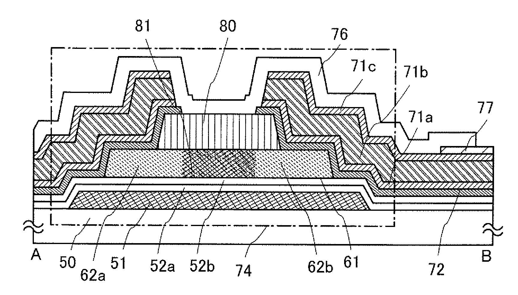
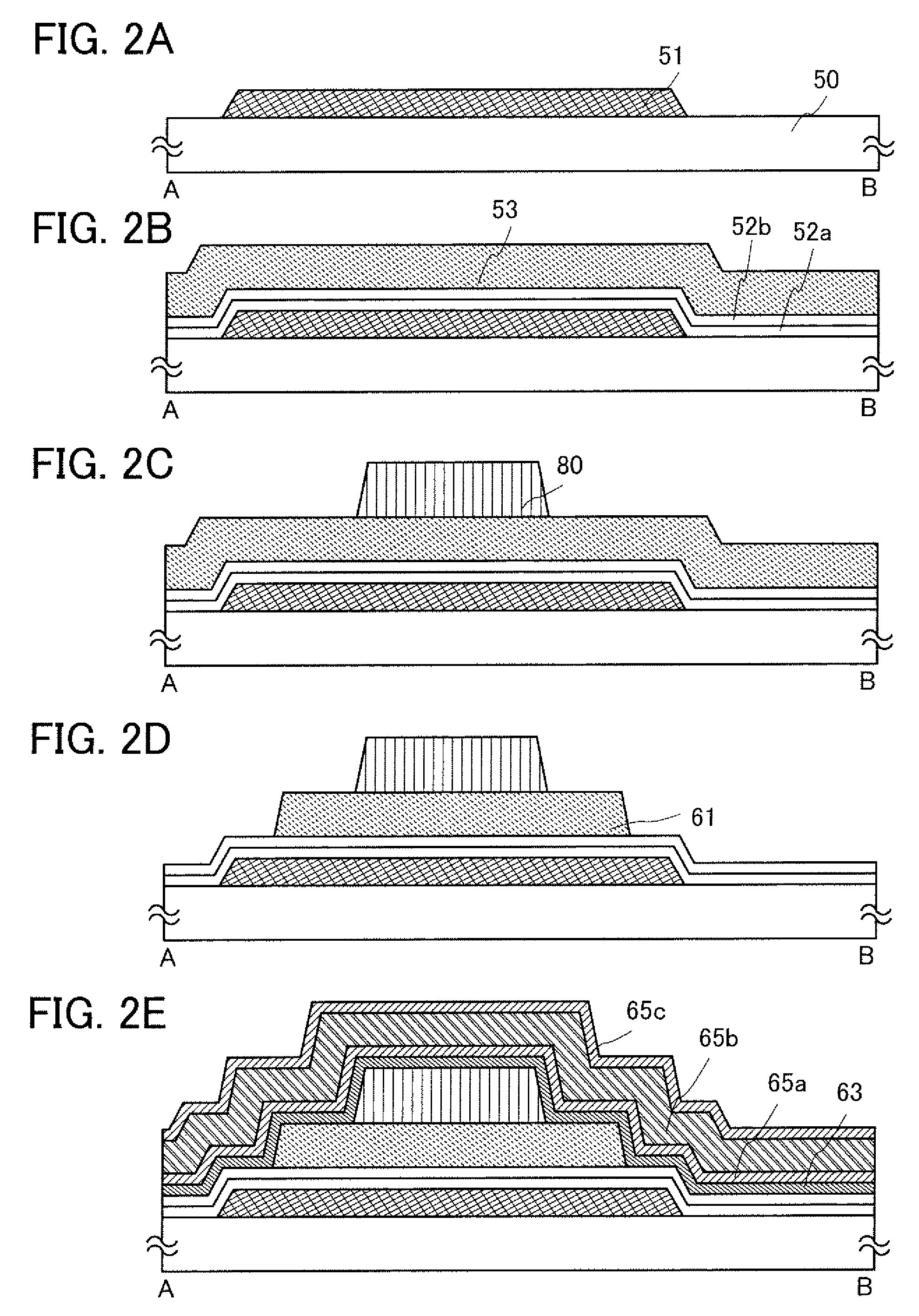
[0053]This embodiment mode describes a thin film transistor used in a display device and a method for manufacturing the thin film transistor, with reference to FIG. 1, FIGS. 2A to 2E, FIGS. 3A to 3C, and FIGS. 4A to 4D. FIG. 1, FIGS. 2A to 2E, and FIGS. 3A to 3C are cross-sectional views showing a thin film transistor and a manufacturing method thereof, and FIGS. 4A to 4D are plan views of a region in which a thin film transistor and a pixel electrode are connected to each other in a pixel. FIG. 1, FIGS. 2A to 2E, and FIGS. 3A to 3C are cross-sectional views showing the thin film transistor taken along a line A-B in FIGS. 4A to 4D and a manufacturing method thereof.

[0054]With regard to a thin film transistor including a microcrystalline semiconductor film, an n-channel thin film transistor has higher mobility than a p-channel thin film transistor, and thus the former is more suitable for a driver circuit. However, either an n-channel or p-channel thin film transistor may be used in ...

embodiment mode 2

[0120]This embodiment mode presents another example in which a thin film transistor has a different shape from that in Embodiment Mode 1. Therefore, parts except for a different part can be made in a similar manner to Embodiment Mode 1, and the same parts or parts having similar functions, or steps for making such parts are not repeatedly described.

[0121]This embodiment mode describes a thin film transistor used in a display device and a method for manufacturing the thin film transistor, with reference to FIG. 5, FIGS. 6A to 6D, and FIG. 15. FIG. 5 and FIG. 15 are cross-sectional views of a thin film transistor and a pixel electrode, and FIGS. 6A to 6D are plan views of a region in which a thin film transistor and a pixel electrode are connected to each other in a pixel. FIG. 5 and FIG. 15 are cross-sectional views showing thin film transistors taken along a line Q-R in FIGS. 6A to 6D and manufacturing steps thereof.

[0122]A channel stop (also referred to as “channel protective”) thi...


PUM


Abstract

A display device including a thin film transistor with high electric characteristics and high reliability, and a method for manufacturing the display device in high yield are proposed. In a display device including a channel stop thin film transistor with an inverted-staggered structure, the channel stop thin film transistor with the inverted-staggered structure includes a microcrystalline semiconductor film including a channel formation region. An impurity region including an impurity element imparting one conductivity type is formed as selected in a region in the channel formation region of the microcrystalline semiconductor film which does not overlap with a source electrode or a drain electrode. In the channel formation region, a non-doped region, to which the impurity element imparting one conductivity type is not added, is formed between the impurity region, which is a doped region to which the impurity element is added, and the source region or the drain region.

Description

BACKGROUND OF THE INVENTION[0001]1. Field of the Invention[0002]The present invention relates to a display device in which a thin film transistor is used at least in a pixel portion, and to a method for manufacturing the display device.[0003]2. Description of the Related Art[0004]In recent years, technology for forming thin film transistors using thin semiconductor films (with thicknesses of from several nanometers to several hundreds of nanometers, approximately) formed over a substrate having an insulating surface has been attracting attention. Thin film transistors are applied to a wide range of electronic devices such as ICs or electro-optical devices, and prompt development of thin film transistors that are to be used as switching elements in image display devices, in particular, is being pushed.[0005]As a switching element in an image display device, a thin film transistor including an amorphous semiconductor film, a thin film transistor including a polycrystalline semiconduct...

Claims


Application Information

Patent Timeline
Patent Type & Authority Patents(United States)
IPC IPC(8): H01L29/04
CPCH01L29/04H01L29/66765H01L29/78696H01L29/41733H01L29/4908
Inventor KOBAYASHI, SATOSHIKAWAMATA, IKUKO
Owner SEMICON ENERGY LAB CO LTD
Why Eureka
Try Eureka