Planar complementary antenna and related antenna array

Active Publication Date: 2021-01-07
CITY UNIVERSITY OF HONG KONG
0 Cites 0 Cited by

AI-Extracted Technical Summary

Problems solved by technology

However, these antennas have ...

Benefits of technology

[0009]In one embodiment of the first aspect, the planar complementary antenna further includes one or more vias extending throug...

Abstract

A planar complementary antenna and an antenna array with multiple planar complementary antennas. The planar complementary antenna has a substrate, a planar dipole antenna arranged on the substrate, a loop antenna arranged on the substrate and operably connected with the planar dipole antenna, and a feed network for connection with a feed source. The feed network is operably connected with the planar dipole antenna and the loop antenna for feeding an electrical signal from the feed source to the planar dipole antenna and the loop antenna so as to form an electric dipole at the planar dipole antenna and a magnetic dipole at the loop antenna.

Application Domain

Simultaneous aerial operationsRadiating elements structural forms +3

Technology Topic

Dipole antennaSelf-complementary antenna +7

Image

  • Planar complementary antenna and related antenna array
  • Planar complementary antenna and related antenna array
  • Planar complementary antenna and related antenna array

Examples

  • Experimental program(1)

Example

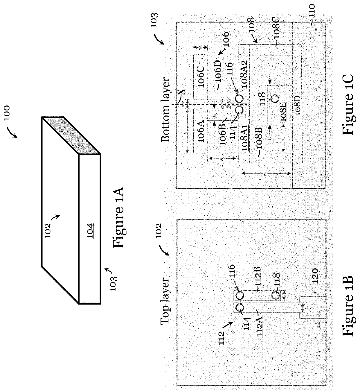
[0055]FIGS. 1A to 1C illustrate a planar complementary wideband antenna 100 in one embodiment of the invention. As shown in FIG. 1A, the antenna 100 includes a substrate 104 and top and bottom layers 102, 103 (FIGS. 1B and 1C respectively) formed on opposite sides of the substrate 104. In this embodiment, the substrate 104 is made from Duroid® 5880 of Rogers Corporation, with a thickness of 0.254 mm.
[0056]The antenna 100 includes a planar dipole antenna 106 and a loop antenna 108 that are operably connected with each other, and a feed network 112 for connection with a feed source. The feed network 112 is operably connected with the planar dipole antenna 106 and the loop antenna 108 for feeding an electrical signal from the feed source to the planar dipole antenna 106 and the loop antenna 108 so as to form an electric dipole at the planar dipole antenna 106 and a magnetic dipole at the loop antenna 108.
[0057]As shown in FIG. 1C, the planar dipole antenna 106 and the loop antenna 108 are both arranged on the same (bottom 103) side of the substrate 104. The planar dipole antenna 106 and the loop antenna 108 are directly connected with each other, i.e., formed integrally.
[0058]The planar dipole antenna 106 has a first portion and a second portion that are symmetric about an axis X. The first and second portions each includes a first elongated conductive strip portion 106A, 106C and a second elongated conductive strip portion 106B, 106D generally extending at an angle to the respective first conductive strip portion 106A, 106C. In this embodiment, the first and second elongated conductive strip portions 106A-106D are generally rectangular (or straight), and the angle between them is about 90 degrees.
[0059]The loop antenna 108 includes a loop-like portion with opposite ends that are close but spaced apart. The loop-like portion includes two generally parallel long sides and two generally parallel short sides. The short sides are generally perpendicular to the long sides. One of the long sides is formed by two elongated conductive strip portions 108A1, 108A2 each connected with a respective half of the planar dipole antenna 106. The elongated conductive strip portions 108A1, 108A2 are generally rectangular (or straight), each being generally perpendicular to the respective second elongated conductive strip portion 106B, 106D. The other long side is formed by an elongated conductive strip portion 108D that is generally rectangular. The short sides are formed by elongated conductive strip portions 108B, 108C that connect the two long sides at respective ends. The elongated conductive strip portions 108B, 108C are generally rectangular. A generally rectangular conductive patch portion 108E is continuous with the elongated conductive strip portion 108D and is arranged within a space defined by the long sides and the short sides. The elongated conductive strip portion 108D is arranged to connect the two short elongated conductive strip portions 108B, 108C such that they are electrically-shorted. The generally rectangular conductive patch portion 108E is arranged to form the ground of the feed network on the opposite (top) side 102 on the substrate 104.
[0060]As shown in FIG. 1C, a ground plane 110 for microstrip line feeding is formed on the bottom side 103 of the antenna 100. In this example, the ground plane 110 is integrally formed with the elongated conductive strip portion 108D and the conductive patch portion 108E.
[0061]Referring now to FIG. 1B, a feed network 112 is formed on the top layer 102. In this example, the feed network 112 is a balun network (balanced to unbalanced feeding network) that transmits an electric signal to the planar dipole antenna 106 and the loop antenna 108. The balun network includes a first conductive strip 112A that provides an input portion for connection with the feed source, and a second conductive strip 112B that provides a phase inverter. As shown in FIG. 1B, the first and second conductive strips 112A, 112B are spaced apart and extending substantially in parallel. The first conductive strip 112A is connected at one end with a microstrip line 120 (50-Ohm in this example), which can be fed by another microstrip line, SMA connector, or other feed sources. The first conductive strip 112A is connected with a via 114 that extends through the substrate 104 to connect with the planar dipole antenna 106 and the loop antenna 108. The second conductive strip 112B is connected with vias 116, 118 at opposite ends. The via 116 connects with the planar dipole antenna 106 and the loop antenna 108; the via 118 connects with the generally rectangular conductive patch portion 108E. The feed network 112 can provide a stable phase shift within a wide operating frequency.
[0062]In operation, the signal from the feed source is transmitted to the portions 106B, 108A1 through the input portion 112A. Also, part of the signal would couple to a slot formed between portions 108A1 and 108E. The signal in the slot would be coupled to the second conductive strip 112B. The signal flow direction in the second conductive strip 112B is opposite to signal flow direction in the first conductive strip 112A so the signals have a 180 degrees phase difference. Then, the signal will be transmitted to portions 106D and 108A2. The input resistance of the antenna loo can be controlled by varying the width L3 of strip 112A.
[0063]The Table below shows exemplary dimensions (in mm and as wavelength fractions) for the antenna structures of FIGS. 1B and 1C for an operating center frequency of 30 GHz.
Parameters L1 L2 L3 L4 L5 Values(mm) 1.5 2.3 0.57 2 0.6 0.15λ 0.23λ 0.06λ 0.2λ 0.06λ Parameters W1 W2 W3 gap gap2 Values(mm) 0.7 1.6 2.8 0.5 0.12 0.07λ 0.16λ 0.28λ 0.05λ 0.01λ
[0064]FIG. 2 show the simulated reflection coefficient and simulated gain as a function of frequency for the antenna of FIGS. 1A to 1C. As shown in FIG. 2, the antenna loo has a wide impedance bandwidth of 69%, with S11
[0065]FIGS. 3A to 3C show simulated radiation patterns for the antenna 100 of FIGS. 1A to 1C at 23 GHz, 30 GHz and 40 GHz respectively. As shown in these Figures, in both E and H planes, the end-fire radiation patterns are stable. Also, low back radiation is observed across the entire operating bandwidth.
[0066]FIGS. 4A and 4B show alternative embodiments of the feed network 212, 312 of the top layer 202, 302. In the embodiment of FIG. 4A, the feed network 212 includes first and second conductive strips 212A, 212B (generally elongated, not straight) operably connected with each other via a common portion 222. Each strip 212A, 212B is connected with a respective via at the terminal end (the bottom layer has corresponding via locations). In the embodiment of FIG. 4B, the feed network 312 includes first and second conductive strips 312A, 312B (generally elongated, not straight) operably connected with each other via a common portion 322. Each of the strips 212A, 212B is connected with a respective via near its open end (the bottom layer has corresponding via locations).
[0067]FIGS. 5A and 5B show an alternative embodiment of the top and bottom layers 402, 403 of the antenna. The main difference between this embodiment and the embodiment of FIGS. 1B and 1C is that the locations of the vias are changed.
[0068]FIGS. 6A and 6B show an alternative embodiment of the top and bottom layers 502, 503 of the antenna. The main differences between this embodiment and the embodiment of FIGS. 1B and 1C are that: (1) the second conductive strip 112B of the feed network 112 on the top side has been moved to the bottom side, as a conductive strip connected directly across the loop antenna, and (2) the vias associated with the second conductive strip 112B are no longer present.
[0069]FIGS. 7A and 7B show an alternative embodiment of the top and bottom layers 602, 603 of the antenna. The main difference between this embodiment and the embodiment of FIGS. 6B and 6C are that the feeding point of the antenna (the location of the via) has changed.
[0070]FIGS. 8A to 8D show different embodiments of the bottom layers 803A-803D of the antenna. In FIG. 8A, as compared with the embodiment of FIG. 1C, the elongated conductive strip portions 108B, 108C are no longer perpendicular to the long sides, but at an angle of less than 90 degrees to the long sides. In FIG. 8B, as compared with the embodiment of FIG. 1C, the elongated conductive strip portions 106A, 106C are no longer perpendicular to the strip portions 106B, 106D, but at an angle of less than 90 degrees to the strip portions 106B, 106D. In FIG. 8C, as compared with the embodiment of FIG. 1C, the elongated conductive strip portions 106A, 106C are no longer rectangular but triangular. In FIG. 8D, as compared with the embodiment of FIG. 1C, the elongated conductive strip portions 108B, 108C are no longer perpendicular to the long sides, but at an angle of less than 90 degrees to the long sides. Also, the elongated conductive strip portions 108B, 108C taper from one long side to the other long side.
[0071]FIG. 9 shows an alternative embodiment of the bottom layer 903 of the antenna. The main difference between this embodiment and the embodiment of FIG. 1C is that the ground plane is now spaced apart from the loop antenna.
[0072]FIGS. 10A and 10B show the top and bottom layers 1002, 1003 of a planar complementary wideband antenna array having multiple complementary wideband antennas in one embodiment of the invention. For simplicity the substrate is not shown. As shown in FIGS. 10A and 10B, the antenna array include multiple planar complementary wideband antennas of like construction as that of FIGS. 1A to 1C. These planar complementary wideband antennas are connected to a common input 1200, and to a common ground plane 1300. In this embodiment, the antennas too are arranged in a 1×4 array structure.
[0073]FIGS. 11A and 11B show an alternative embodiment of the top and bottom layers 1102, 1103 of the antenna. The main difference between this embodiment and the embodiment of FIGS. 1B and 1C is that in this embodiment the dipole antenna is formed on the top layer and connected with the feed network on the top layer. In other words, the planar dipole antenna and the loop antenna are arranged on opposite sides of the substrate.
[0074]The antennas and antenna arrays as provided in the above embodiments have excellent electrical parameters such as wide operating bandwidth, low back radiation, and are stable in gain and radiation pattern shape over the frequency bandwidth. In particular, the wide operating bandwidth makes it highly attractive for the development of various kinds of indoor and outdoor base station antennas for modern cellular communication systems. The antenna has a simple structure and therefore can be made cheaply. The antenna can be used as a basic element in the design of low-cost high-performance antenna arrays with different gain and beam widths. The above embodiments have provided a planar complementary antenna that includes a planar dipole antenna and a loop antenna. Various feed networks, e.g., balun networks, differential input networks, etc., can be used to excite the antenna. The planar complementary wideband has low back radiation, stable gain, and a stable radiation pattern shape. The antenna embodiments disclosed have one or more of the following advantages: small size, wide bandwidth, good electric performance, low fabrication cost, and simple structure.
[0075]It will be appreciated by persons skilled in the art that numerous variations and/or modifications may be made to the invention as shown in the specific embodiments without departing from the spirit or scope of the invention as broadly described. Positional terms “top”, “bottom”, “above”, “below”, “horizontal”, “vertical”, and the like are used for illustration only; they are not intended to limit the orientation of the apparatus or device. The described embodiments of the invention should therefore be considered in all respects as illustrative, not restrictive.
[0076]For example, the planar dipole antenna can take a different form, preferably symmetric. The loop antenna can take a different form. The planar dipole antenna, the loop antenna, and the feed network can be formed with (but not limited to) conductive materials in the form of, e.g., strips, patches, etc., directly or indirectly connected with each other. The loop antenna need not include spaced-apart opposite ends. The loop antenna need not be a single-loop antenna. The loop antenna can be a loop antenna of different form, shape, and size, with a complete closed loop or the form of a near complete loop. The ground plane can be formed integrally with the loop antenna or the ground plane may be spaced apart from the loop antenna. The feed network can be a differential feed network instead of a balun network. The differential feed network can be arranged on the same side as the balun network. The differential feed network may include two input portions each arranged to receive a respective input signal (the two input signals being out of phase). The number, size, and position of vias can be varied, so long as they operably connect the planar dipole antenna, the loop antenna, and the feed network. The planar complementary antenna is particularly adapted for (but not limited to) operation at GHz and THz frequencies.
[0077]For example, the antenna array can be formed with different number of planar complementary antennas. The planar complementary antennas can be of different form, size, shape, and configuration. The antenna array is particularly adapted for (but not limited to) operation at GHz and THz frequencies.
[0078]The planar complementary antenna and related antenna array may be formed from a PCB substrate using, e.g., conventional PCB fabrication techniques.

PUM

no PUM

Description & Claims & Application Information

We can also present the details of the Description, Claims and Application information to help users get a comprehensive understanding of the technical details of the patent, such as background art, summary of invention, brief description of drawings, description of embodiments, and other original content. On the other hand, users can also determine the specific scope of protection of the technology through the list of claims; as well as understand the changes in the life cycle of the technology with the presentation of the patent timeline. Login to view more.
Why Eureka
Try Eureka