Methods for selective deposition utilizing n-type dopants and/or alternative dopants to achieve high dopant incorporation

a selective deposition and dopant technology, applied in the direction of coatings, semiconductor devices, chemical vapor deposition coatings, etc., can solve the problem of difficult layer formation

Active Publication Date: 2021-02-04
ASM IP HLDG BV
View PDF9 Cites 155 Cited by
  • Summary
  • Abstract
  • Description
  • Claims
  • Application Information

AI Technical Summary

Benefits of technology

[0006]This summary is provided to introduce a selection of concepts in a simplified form. These concepts are described in further detail in the detailed description of example embodiments of the disclosure below. This summary is not intended to identify key features or essential features of the claimed subject matter, nor is it intended to be used to limit the scope of the claimed subject matter.
[0007]A method for forming a contact layer is disclosed. The method may comprise: cleaning a device on a semiconductor substrate of any oxides, the semiconductor substrate being disposed on a susceptor in a reaction chamber; stabilizing a temperature of the reaction chamber; flowing a halide precursor onto the device, the halide precursor comprises at least one of: hydrogen fluoride (HF); hydrogen chloride

Problems solved by technology

Formation of the layers may be difficult when growing on a substitutional lattice site.
There may be issues that may res

Method used


Image

  • Methods for selective deposition utilizing n-type dopants and/or alternative dopants to achieve high dopant incorporation
  • Methods for selective deposition utilizing n-type dopants and/or alternative dopants to achieve high dopant incorporation
  • Methods for selective deposition utilizing n-type dopants and/or alternative dopants to achieve high dopant incorporation

Examples


Embodiment Construction

[0013]Although certain embodiments and examples are disclosed below, it will be understood by those in the art that the invention extends beyond the specifically disclosed embodiments and / or uses of the invention and obvious modifications and equivalents thereof. Thus, it is intended that the scope of the invention disclosed should not be limited by the particular disclosed embodiments described below.

[0014]The illustrations presented herein are not meant to be actual views of any particular material, structure, or device, but are merely idealized representations that are used to describe embodiments of the disclosure.

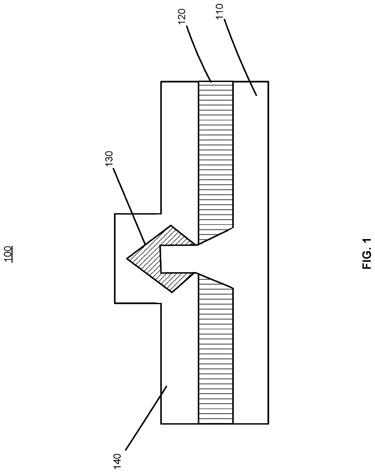
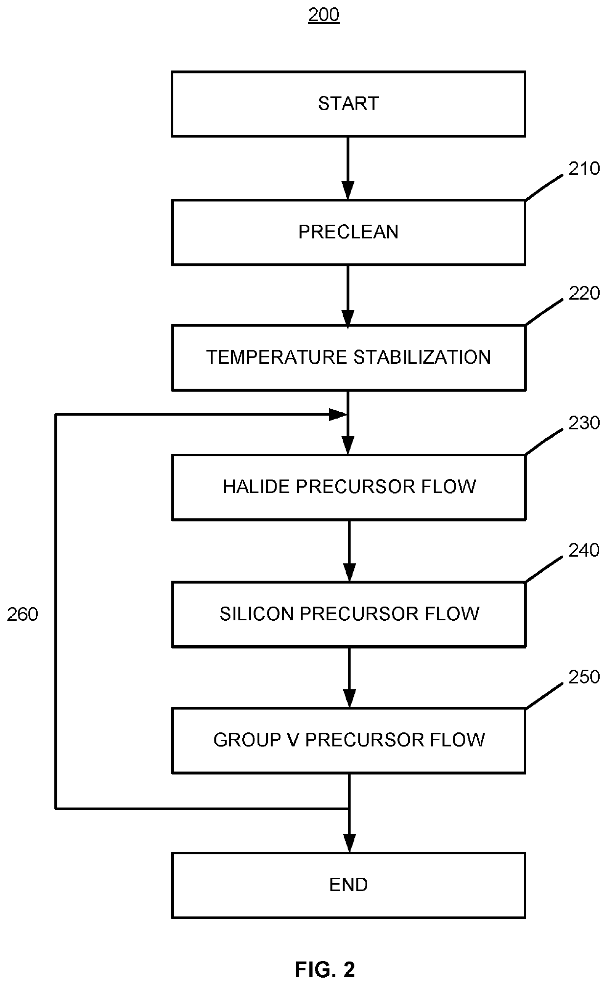
[0015]For FinFET applications, a contact layer may be needed on top of a Fin. Contact layers may also be grown for silicon germanium (SiGe) applications as well. For contact layers in particular NMOS applications, it may be desirable to incorporate high levels of n-type dopant. Such may increase the electrically active behavior of the contact layer.

[0016]FIG. 1 illustr...


PUM

PropertyMeasurementUnit
Temperatureaaaaaaaaaa

Abstract

A method for forming a doped layer is disclosed. The doped layer may be used in a NMOS or a silicon germanium application. The doped layer may be created using an n-type halide species in a n-type dopant application, for example.

Description

FIELD OF INVENTION[0001]This application is a non-provisional of, and claims priority to and the benefit of, U.S. Provisional Patent Application No. 62 / 879,980, filed Jul. 29, 2019 and entitled “METHODS FOR SELECTIVE DEPOSITION UTILIZING N-TYPE DOPANTS AND / OR ALTERNATIVE DOPANTS TO ACHIEVE HIGH DOPANT INCORPORATION,” which is hereby incorporated by reference herein.FIELD OF INVENTION[0002]The present disclosure generally relates to selective deposition of semiconductor films on substrates. More particularly, the disclosure relates to selective deposition utilizing dopants. The dopant precursors may include hydrides and halogenated Group V.BACKGROUND OF THE DISCLOSURE[0003]For logic applications, FinFET transistors have been made by epitaxial deposition processes. Dopants have been used to match a particular channel type, such as an n-type doped layer for NMOS applications. Particular n-type layers formed may include silicon carbide (SiC), silicon carbophosphine (SiCP), and silicon p...

Claims


Application Information

Patent Timeline
IPC IPC(8): H01L21/02H01L29/08H01L29/66C23C16/458C23C16/02C23C16/30
CPCH01L21/02576H01L21/02661H01L29/0847H01L29/66795H01L21/02532H01L21/0262C23C16/4583C23C16/0227C23C16/30H01L21/02609H01L21/02639H01L21/228H01L21/02381H01L21/0243C23C16/04C23C16/325H01L21/28518H01L21/823431H01L21/823475H01L21/02068C23C16/24C23C16/52C23C16/22C23C16/44C23C16/46C23C16/0209C23C16/455
Inventor TOLLE, JOHNMARGETIS, JOEKOHEN, DAVID
Owner ASM IP HLDG BV
Why Eureka
Try Eureka