Structures including dielectric layers and methods of forming same
a technology of dielectric layers and dielectric layers, applied in the direction of coatings, chemical vapor deposition coatings, metallic material coating processes, etc., can solve the problems of relatively porous amorphous film deposition, low k value of dielectric material deposition using pecvd, and film having undesirably low elastic modulus
- Summary
- Abstract
- Description
- Claims
- Application Information
AI Technical Summary
Benefits of technology
Problems solved by technology
Method used
Image

Examples
example 1
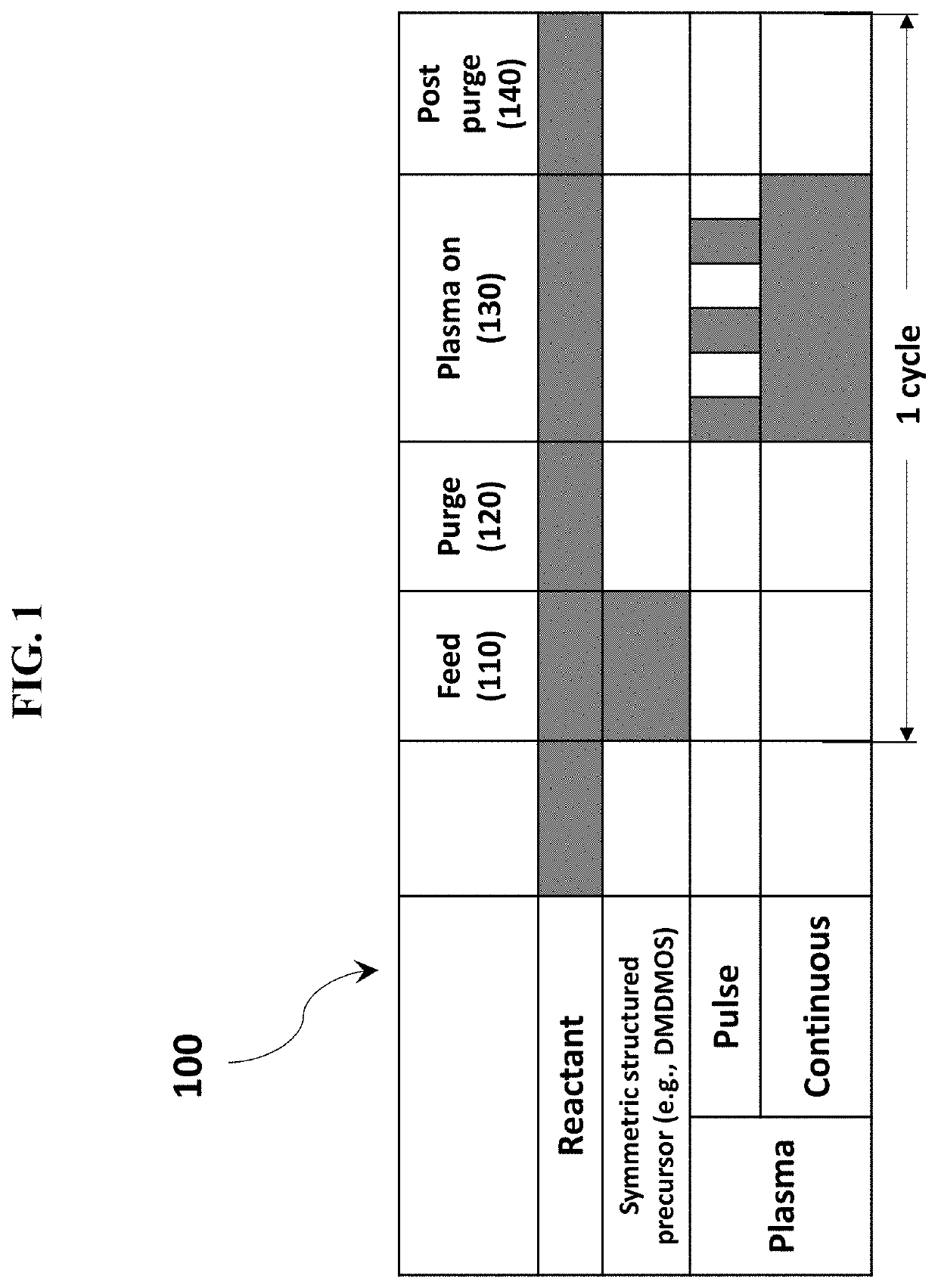
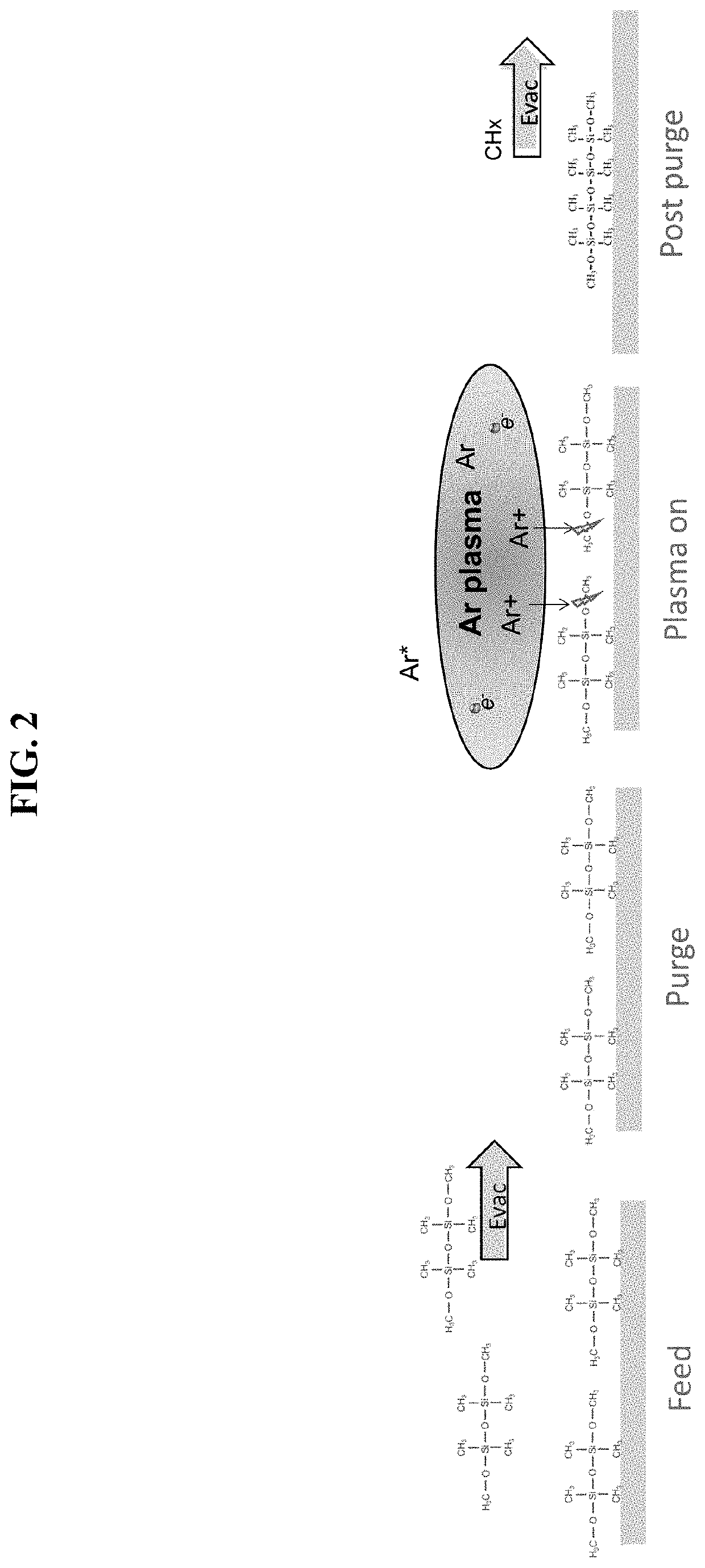
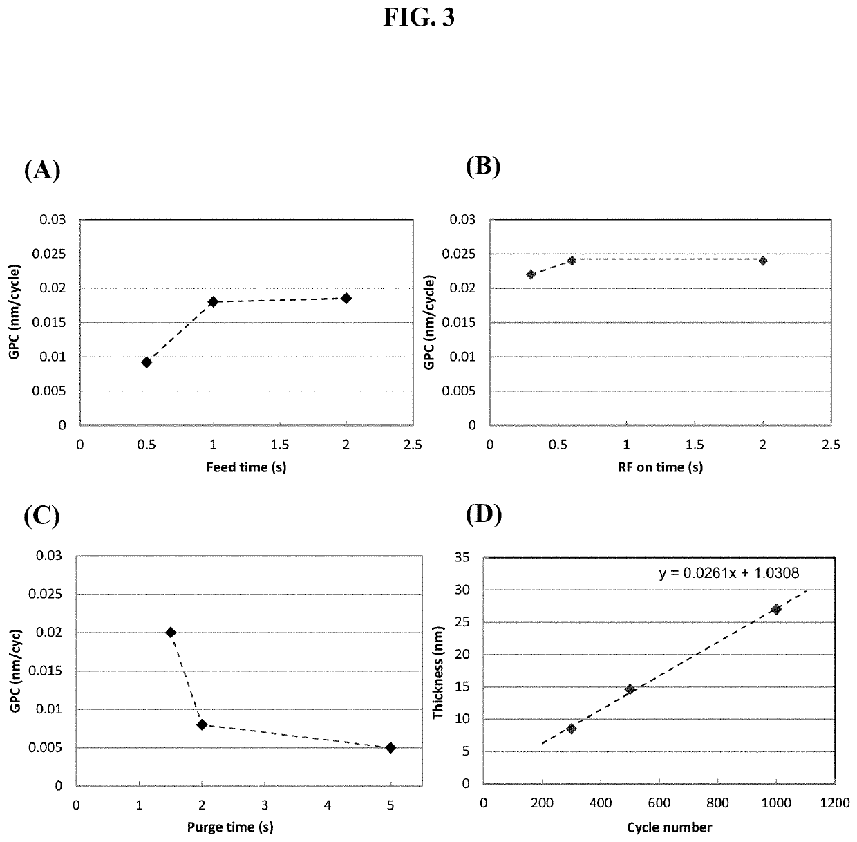
[0046]A low-k film was formed by PEALD on a substrate in accordance with the process illustrated in FIGS. 1 and 2. The cycle was performed using a continuous plasma step. FIG. 3 illustrates that the methods of the present disclosure result in ALD-like film growth. FIG. 3A is a graph showing the relationship between growth per cycle (GPC) (nm / cycle) and precursor feed time (seconds), indicating that the growth reached a saturation point after 1 second of feed time. FIG. 3B shows the relationship between GPC and RF on time (seconds), indicating that the growth reached a saturation point after approximately 0.6 seconds of plasma on time. FIG. 3C shows the relationship between GPC and purge time (seconds), indicating that a purge is substantially complete at about 2 seconds. After about 2 seconds, mainly surface reactions are contributing to the GPC. FIG. 3D shows the relationship between thickness of the film (nm) and the number of cycles repeated in the deposition process. FIG. 3D ind...
example 2
[0047]FIGS. 4A and 4B illustrate Fourier Transform Infrared (FTIR) spectrums of Si—CH3 films formed under different process conditions according to embodiments of the disclosure. Under process conditions of 1000 Pa pressure, 200 W power, and 2 seconds, the k value is about 4. Under 1000 Pa pressure, 200 W power, and 0.3 seconds, the k value is about 4. Under 3000 Pa pressure, 100 W power, and 0.15 seconds, the k value is 3.1. The improved k value under these conditions is a further improvement over the conventional PECVD method (reference), exhibiting a k value of 3.23. The Si—CH3 peaks increase when plasma ion energies are decreased. This is achieved by increasing the pressure, decreasing the power, and decreasing the plasma on time, keeping the original Si—CH3 structure in the precursor.
[0048]FIG. 5 illustrates FTIR spectrums of Si—CH3 films formed using pulsed plasma vs continuous plasma under the optimal conditions determined in FIG. 4, specifically 3000 Pa pressure, 100 W power...
PUM
| Property | Measurement | Unit |
|---|---|---|
| Temperature | aaaaa | aaaaa |
| Temperature | aaaaa | aaaaa |
| Temperature | aaaaa | aaaaa |
Abstract
Description
Claims
Application Information
 - R&D
- Intellectual Property
- Life Sciences
- Materials
- Tech Scout
- Unparalleled Data Quality
- Higher Quality Content
- 60% Fewer Hallucinations
Browse by: Latest US Patents, China's latest patents, Technical Efficacy Thesaurus, Application Domain, Technology Topic, Popular Technical Reports.
© 2025 PatSnap. All rights reserved.Legal|Privacy policy|Modern Slavery Act Transparency Statement|Sitemap|About US| Contact US: help@patsnap.com