Optical Shuffle Computation Network

a computation network and optical shuffle technology, applied in electromagnetic transmission, electrical equipment, electromagnetic network arrangements, etc., can solve the problems of computational systems growing in complexity, increasing the space of wires on the system, and increasing the limitations of computation systems, and achieve high memory density

Active Publication Date: 2021-03-18
FATHOM RADIANT PBC
View PDF0 Cites 0 Cited by
  • Summary
  • Abstract
  • Description
  • Claims
  • Application Information

AI Technical Summary

Benefits of technology

[0009]The present invention provides an optical network that allows effective routing of signals between collected arrays of ports and dispersed arrays of ports on electronic computing chips (reversibly, also between the dispersed arrays and the collected arrays).
[0025]It is desirable to build the optical transducers as telecentric, high-numerical aperture modulators or emitters, since this allows the highest density of signal channels. It is also desirable to provide a transversely compact optical system constituting the lenslet for each tile, so that the lenslet array to collimate the optical signals, and the lenslet array to focus the optical signals remain compact, and consequently allow that the dead space between the tiles remains small. It is also desirable to provide a transversely compact optical system for routing the optical signals between the collimating lenslets and the focusing lenslets, so that multiple free-space optical trains addressing their own arrays of tiles may be laid side to side and connected electronically with short electrical interconnects.

Problems solved by technology

Computational systems are increasingly limited by the wires used to interconnect processing elements.
These wires consume more space on the system as the computational systems grow in complexity.
Efforts to utilize optical waveguides provide high speed optical interconnects, but these cannot easily provide a number of channels which scales with chip area, since the channels usually exit the chip edge.
However large, configurable exchange subnetworks have significant complexity in themselves, because an exchange network with full degrees of freedom is combinatorially complex.
Additionally, optical shuffle networks, to date, have not been developed with density comparable to the available space-bandwidth product of the optical system, due to underfilled subarrays in the shuffle, and systems that can't be tiled into larger networks.

Method used


Image

  • Optical Shuffle Computation Network
  • Optical Shuffle Computation Network
  • Optical Shuffle Computation Network

Examples


Embodiment Construction

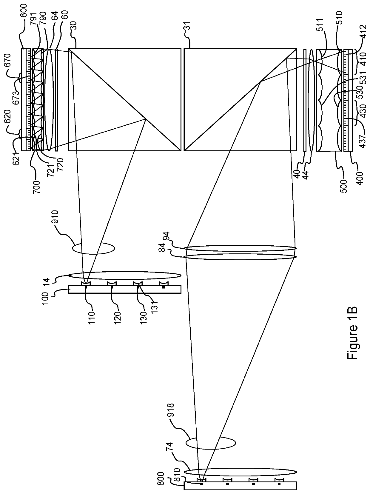
[0039]The following description sets forth embodiments of an optical shuffle computation network according to the invention. Embodiments of the invention can be applied to computational environments such as artificial neural network systems, array computation, memory access and to networked computational systems.

[0040]The general functionality of the optical shuffle computation network is to accept signals from an array of collected tiles, transmit signals from each over a long range to a set of dispersed tiles, where the signals may access memory and where the signals may be exchanged locally and transmitted back to the original or to an exchanged collected tile.

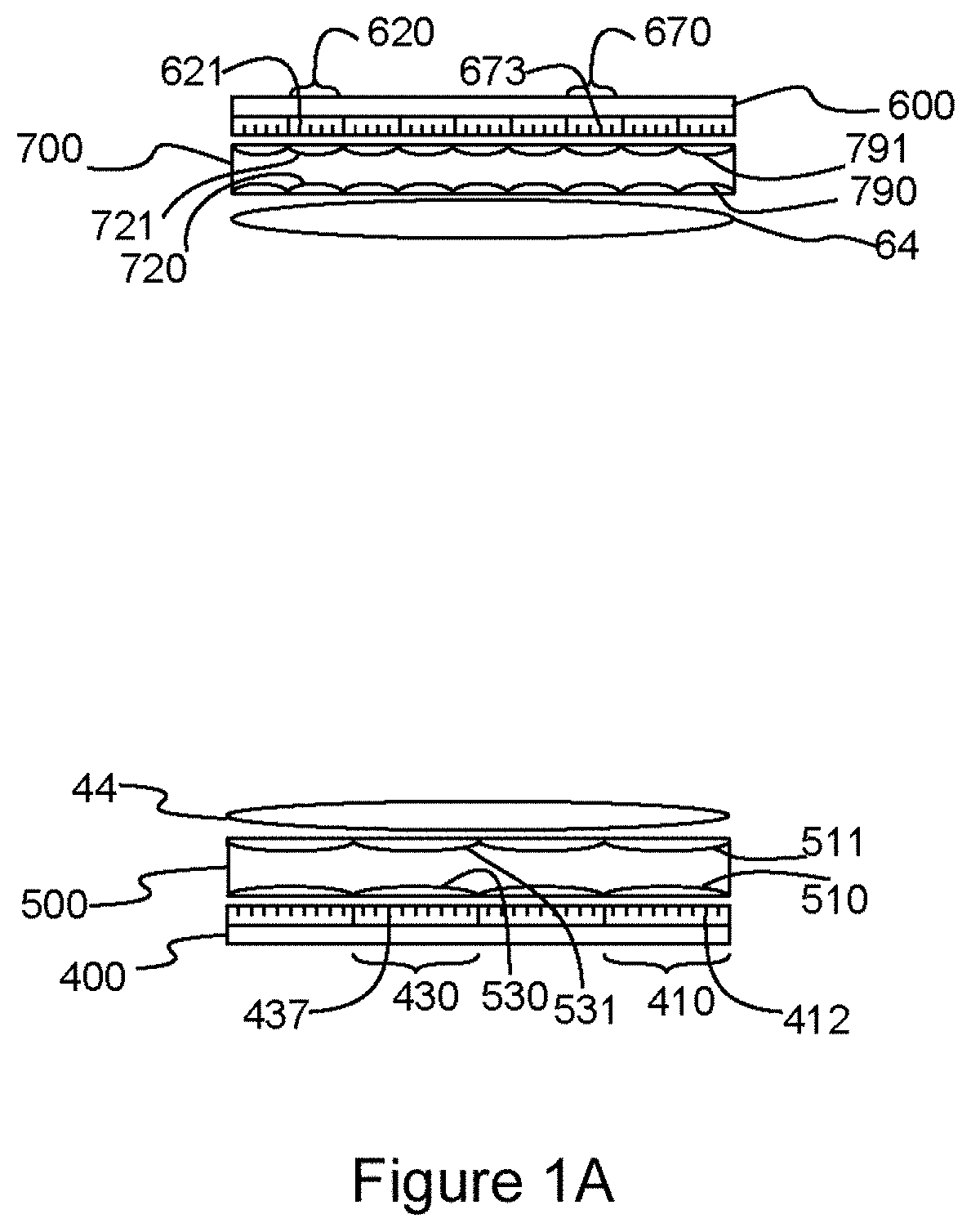
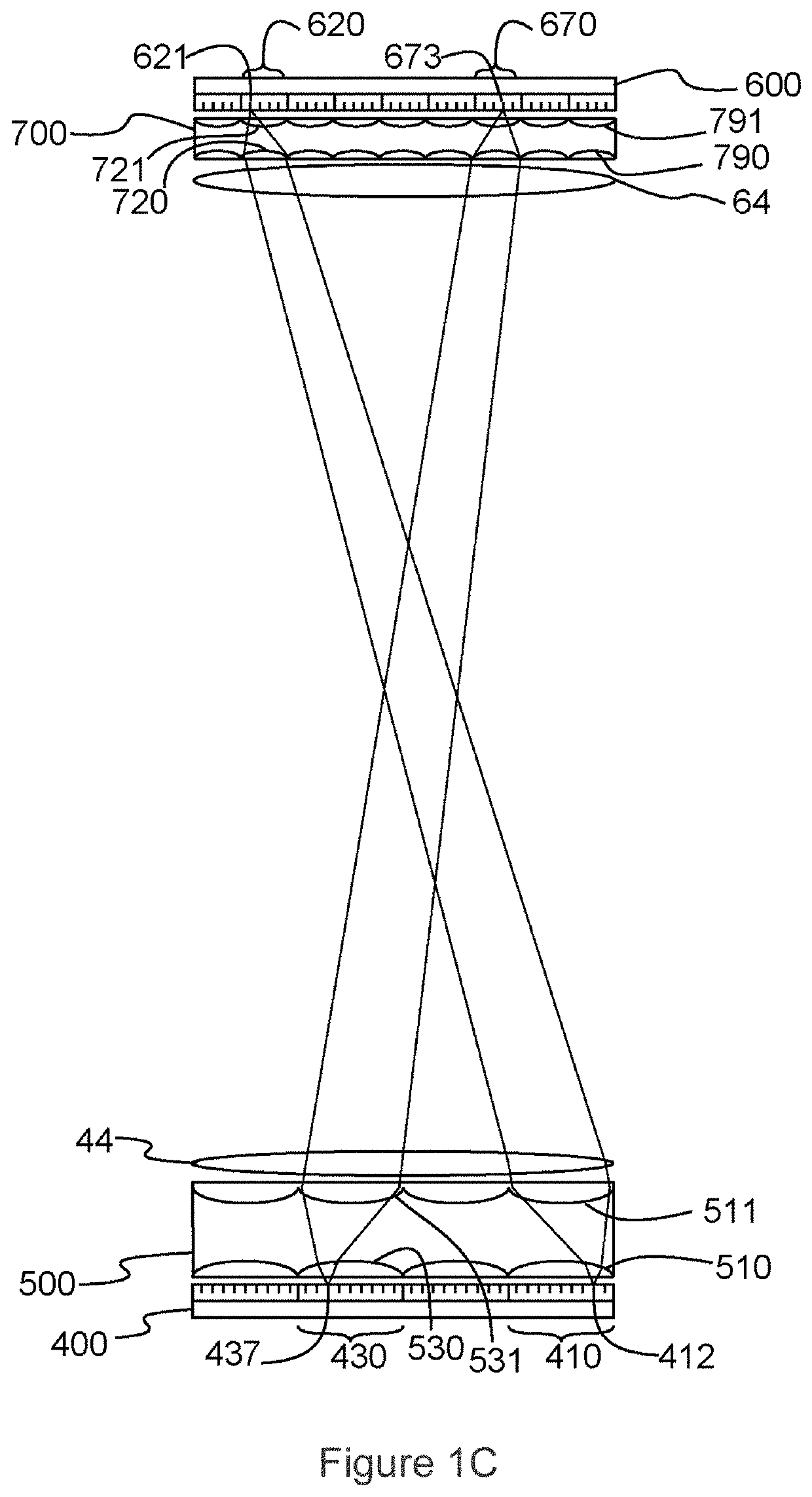
[0041]FIGS. 1A-1E are schematic top views of an optical shuffle-exchange network according to an embodiment of the invention. FIG. 1A shows communication between optoelectronic transducer arrays 400 and 600. In the specific embodiment shown in FIGS. 1A-1E, collected array 400 is a portion of the originating chip (not shown)...


PUM


Abstract

Optical communication system communicates between an array of originating tiles and an array of terminating tiles. Each array is associated with a lenslet array, such as a two-layer array which has two layers of lenslets. Each originating tile has an array of transmitters and each terminating tile has an array of receivers. Each tile is associated with a common lenslet or lenslet pair. A beamlet from a representative transmitter passes through the lenslet pair adjacent to its tile to become a collimated beam whose angle is related to the location of the transmitter. The collimated beam passes through the receiver lenslet pair adjacent to the tile containing the receiver associated with the representative transmitter, and is focused onto that receiver by that lenslet pair. The system may operate in the reverse direction, wherein the transmitters are transmitter-receivers, the receivers are receiver-transmitters, and a beam from a receiver-transmitter is directed to its corresponding transmitter-receiver.

Description

BACKGROUND OF THE INVENTIONField of the Invention[0001]This application relates generally to optical systems for communication in computational systems, and more specifically to techniques and devices for computing with shuffle-exchange systems using optical systems to perform the shuffle.Discussion of Related Art[0002]Computational systems are increasingly limited by the wires used to interconnect processing elements. The signal delay for the longer wires dominates the gate delay. These wires consume more space on the system as the computational systems grow in complexity. And as the feature size is made smaller, the power dissipated by a long-distance wire dominates the power required for a gate.[0003]The on-chip long-wire interconnect requires buffered segments to overcome a delay which otherwise grows quadratically with wire length. With periodic buffering, the delay and power required for a wired interconnect still grow linearly with interconnect length.[0004]The industry is se...

Claims


Application Information

Patent Timeline
Patent Type & Authority Applications(United States)
IPC IPC(8): H04B10/27H04B10/516
CPCH04B10/27H04B10/516H04B10/803
Inventor AUSTIN, DANE R.ANDREGG, WILLIAMNELSON, ERIK C.WEVERKA, ROBERT T.
Owner FATHOM RADIANT PBC
Why Eureka
Try Eureka