
Atomic layer etching of metals

a technology of atomic layer and metal, which is applied in the direction of basic electric elements, semiconductor/solid-state device manufacturing, electric devices, etc., can solve the problems of fragile substrates becoming damaged, additional processing capabilities,

Active Publication Date: 2021-03-25
APPLIED MATERIALS INC
View PDF0 Cites 2 Cited by
  • Summary
  • Abstract
  • Description
  • Claims
  • Application Information

AI Technical Summary

Benefits of technology

The present patent describes methods for selectively etching copper, cobalt, and / or aluminum layers on semiconductor devices. The methods involve oxidizing the surface of the metal layers and reacting them with hexafluoroacetylacetonate vapor to form a volatile compound which is then pumped out of the chamber. The result is a selective atomic layer etching of the metal surface, with minimal damage to the surrounding materials. The methods provide precise and efficient means for fabricating semiconductor devices with copper, cobalt, or aluminum layers.

Problems solved by technology

Reliably producing sub-half micron and smaller features are one of the key technology challenges for next generation very large-scale integration (VLSI) and ultra-large-scale integration (ULSI) of semiconductor devices.
However, as the limits of circuit technology are pushed, the shrinking dimensions of VLSI and ULSI technology have placed additional demands on processing capabilities.
Additionally, conventional etchants have low selectivity to etch one material over another material present in the structure, which may result in a fragile substrate becoming damaged when etching interconnection structures.

Method used


Image

  • Atomic layer etching of metals
  • Atomic layer etching of metals
  • Atomic layer etching of metals

Examples


Embodiment Construction

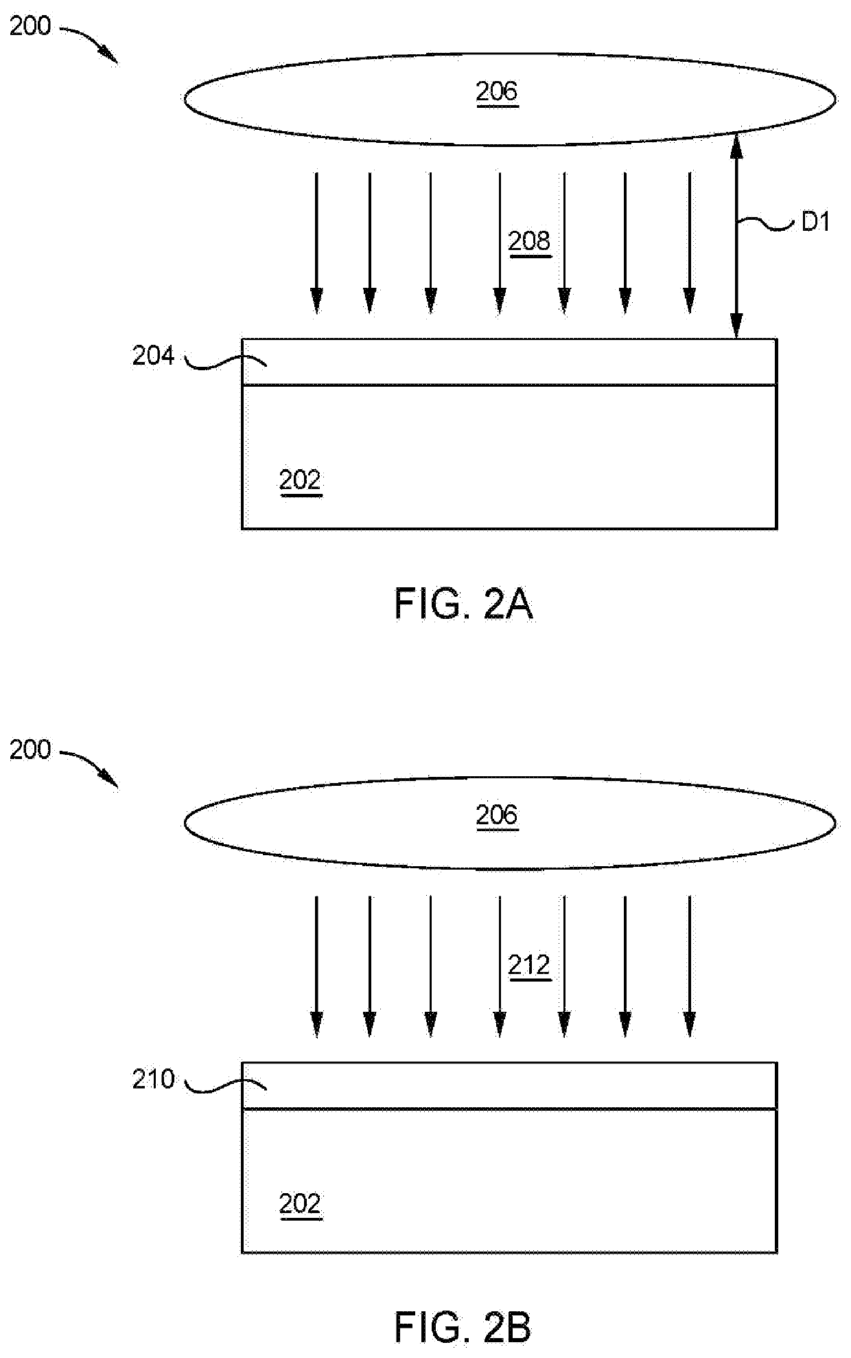
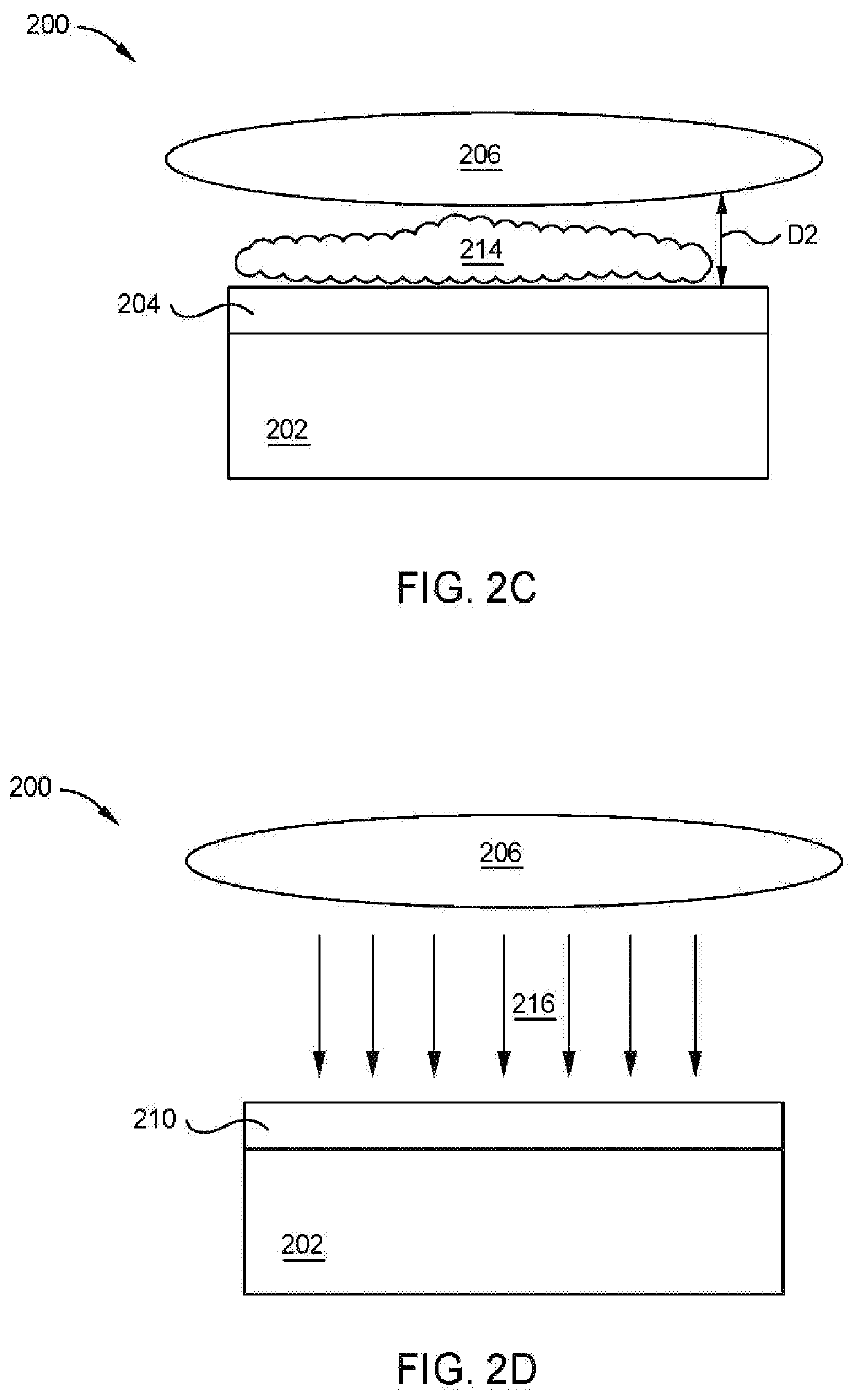
[0016]The present disclosure generally relates to methods for selectively etching copper, cobalt and / or aluminum layers on a substrate semiconductor manufacturing applications. A substrate comprising one or more copper layers, cobalt layers, or aluminum layers is transferred to a processing chamber. The surface of the copper, cobalt, or aluminum layer is oxidized. The oxidized copper, cobalt, or aluminum surface is then exposed to hexafluoroacetylacetonate vapor. The hexafluoroacetylacetonate vapor reacts with the oxidized copper, cobalt, or aluminum surface to form a volatile compound, which is then pumped out of the chamber. The reaction of the oxidized copper, cobalt, or aluminum surface with the hexafluoroacetylacetonate vapor selectively atomic layer etches the copper, cobalt, or aluminum surface.

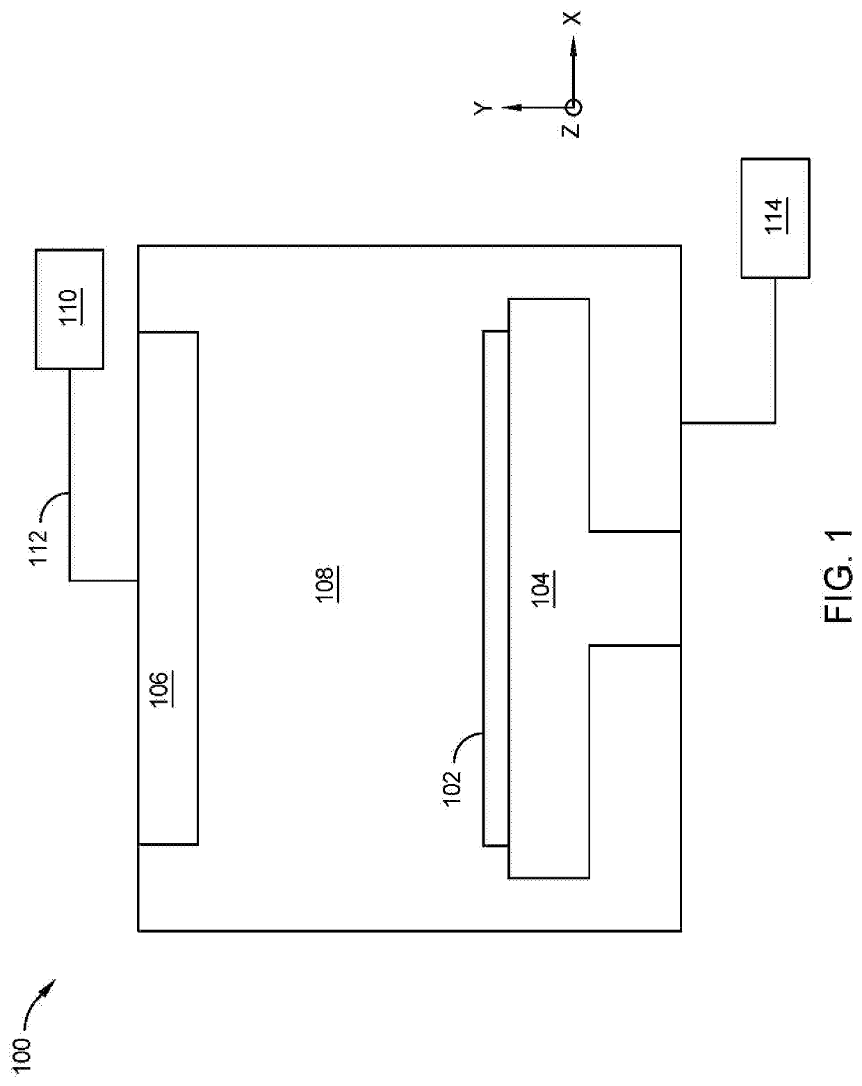
[0017]FIG. 1 illustrates an exemplary process chamber 100 utilized for atomic layer etching (ALE) layers on a substrate 102, according to one embodiment. The processing chamber 100 com...


PUM

PropertyMeasurementUnit
temperatureaaaaaaaaaa
thicknessaaaaaaaaaa
thicknessaaaaaaaaaa

Abstract

The present disclosure generally relates to methods for selectively etching copper, cobalt, and / or aluminum layers on a substrate semiconductor manufacturing applications. A substrate comprising one or more copper layers, cobalt layers, or aluminum layers is transferred to a processing chamber. The surface of the copper, cobalt, or aluminum layer is oxidized. The oxidized copper, cobalt, or aluminum surface is then exposed to hexafluoroacetylacetonate vapor. The hexafluoroacetylacetonate vapor reacts with the oxidized copper, cobalt, or aluminum surface to form a volatile compound, which is then pumped out of the chamber. The reaction of the oxidized copper, cobalt, or aluminum surface with the hexafluoroacetylacetonate vapor selectively atomic layer etches the copper, cobalt, or aluminum surface.

Description

CROSS-REFERENCE TO RELATED APPLICATIONS[0001]This application claims benefit of Indian provisional patent application serial number 201941037780, filed Sep. 19, 2019, which is herein incorporated by reference.BACKGROUNDField[0002]Embodiments of the present disclosure generally relate to methods for selectively etching copper, cobalt, and / or aluminum layers on a substrate for semiconductor manufacturing applications.Description of the Related Art[0003]Reliably producing sub-half micron and smaller features are one of the key technology challenges for next generation very large-scale integration (VLSI) and ultra-large-scale integration (ULSI) of semiconductor devices. However, as the limits of circuit technology are pushed, the shrinking dimensions of VLSI and ULSI technology have placed additional demands on processing capabilities. As circuit densities increase for next generation devices, the widths of interconnects, such as vias, trenches, contacts, gate structures and other featu...

Claims


Application Information

Patent Timeline
Patent Type & Authority Applications(United States)
IPC IPC(8): H01L21/3213H01L21/768
CPCH01L21/32136H01L21/76886H01L21/32135H01L21/30655H01L21/31056H01L21/30604H01L21/322
Inventor DEEPAK, NITINGORADIA, PRERNA SONTHALIA
Owner APPLIED MATERIALS INC
Learn More