Nonvolatile memory device with address re-mapping

Active Publication Date: 2021-04-01
SAMSUNG ELECTRONICS CO LTD
View PDF0 Cites 2 Cited by
  • Summary
  • Abstract
  • Description
  • Claims
  • Application Information

AI Technical Summary

Benefits of technology

The patent describes a way to make nonvolatile memory devices that are smaller and perform better. The method involves organizing the memory blocks into groups based on their physical and electrical characteristics. If there is a defect in one group, the memory blocks in a different group can be re-mapped to replace the defective ones. This helps to make the chip size smaller while maintaining its performance.

Problems solved by technology

As memory cell sizes decrease to achieve high integration, the complexity of the structures of operation circuits and / or wirings included in the memory devices can degrade the memory cell electrical characteristics.

Method used


Image

  • Nonvolatile memory device with address re-mapping
  • Nonvolatile memory device with address re-mapping
  • Nonvolatile memory device with address re-mapping

Examples


Embodiment Construction

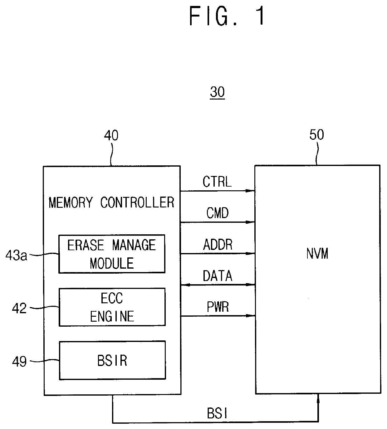
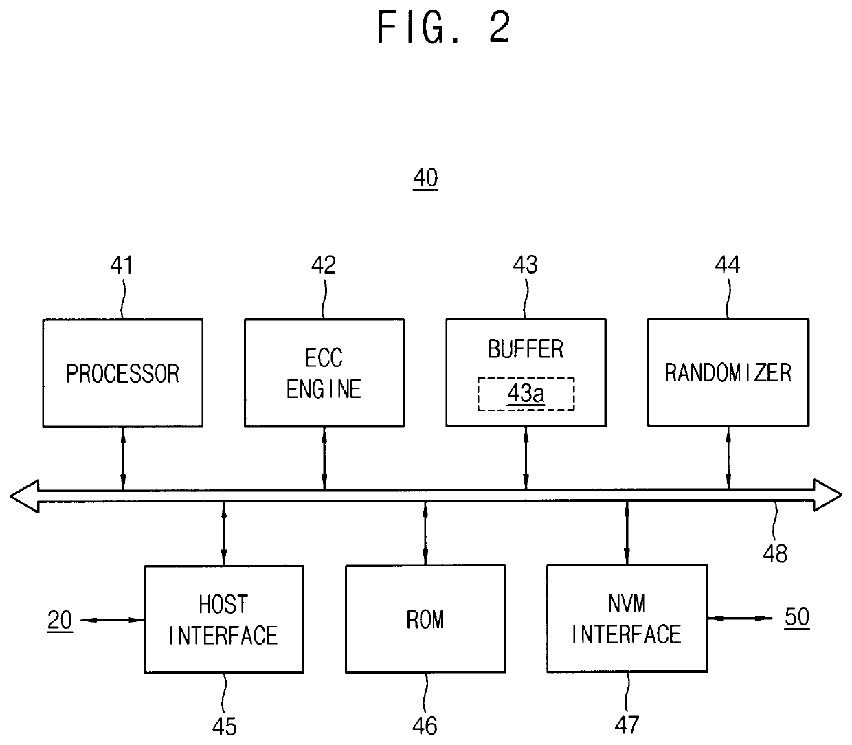
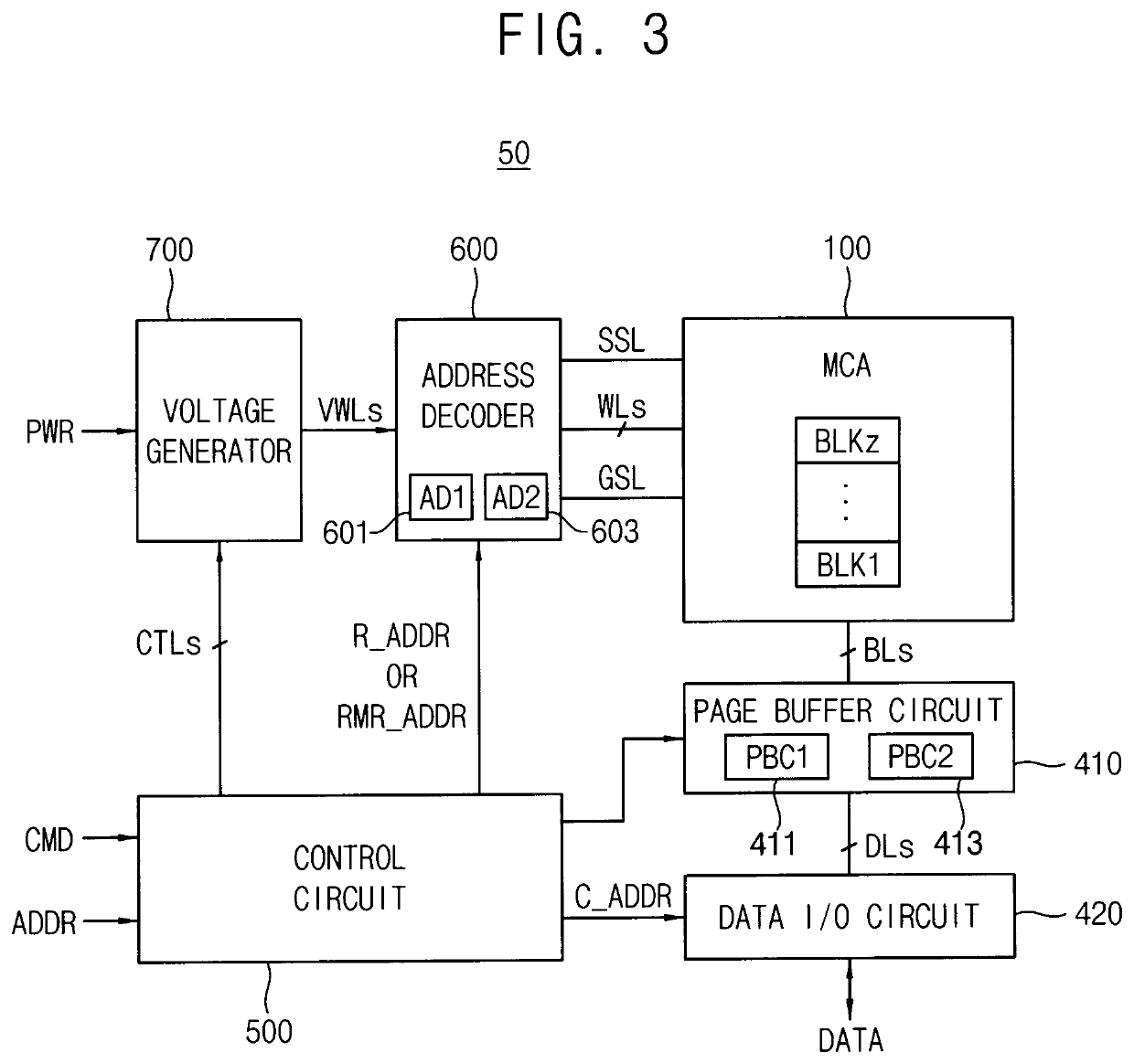
[0036]Various exemplary embodiments will be described more fully hereinafter with reference to the accompanying drawings, in which some exemplary embodiments are shown.

[0037]The embodiments are described, and illustrated in the drawings, in terms of functional blocks, units and / or modules. These blocks, units and / or modules may be physically implemented by electronic (or optical) circuits such as logic circuits, discrete components, microprocessors, hard-wired circuits, memory elements, wiring connections, and the Ike, which may be formed together in a single integrated circuit (e.g., as a single semiconductor chip) or as separate integrated circuits and / or discrete components (e.g., several semiconductor chips wired together on a printed circuit board) using semiconductor fabrication techniques and / or other manufacturing technologies. These blocks, units and / or modules may be implemented by a processor (e.g., a microprocessor, a controller, a CPU, a GPU) or processors that are prog...


PUM


Abstract

A nonvolatile memory device includes memory cell region including a first metal pad and a peripheral circuit region including a second metal pad, is connected to the memory cell region by the first metal pad and the second metal pad and includes including an address decoder and a page buffer circuit located on a first substrate. A memory cell array is provided in the memory cell region, which includes a first vertical structure on a second substrate. The first vertical structure includes first sub-blocks and first via areas in which one or more through-hole vias are provided, and through-hole vias pass through the first vertical structure. A control circuit in the peripheral circuit region groups the memory blocks into a plurality of groups based on whether the memory blocks is close to the first via areas and performs address re-mapping.

Description

REFERENCE TO RELATED APPLICATION[0001]This application is a continuation-in-part of U.S. patent application Ser. No. 16 / 865,948, filed May 4, 2020, which claims priority under 35 USC § 119 to Korean Patent Application No. 10-2019-0119935, filed Sep. 27, 2019, the disclosures of which are hereby incorporated herein by reference.BACKGROUND1. Technical Field[0002]Exemplary embodiments relate generally to memory devices, and more particularly to nonvolatile memory devices2. Discussion of the Related Art[0003]Semiconductor memory devices may be volatile or nonvolatile. Flash memory devices are typically nonvolatile semiconductor memory devices. Flash memory devices may be used as a voice and image data storing medium for information appliances, such as computers, cellular phones, PDAs, digital cameras, handheld PCs, and the like.[0004]Recently, nonvolatile memory devices having memory cells that are stacked in three dimensions have been researched to improve integration of the nonvolatil...

Claims


Application Information

Patent Timeline
IPC IPC(8): G11C29/00G11C7/10G11C29/18G11C29/44G11C29/12
CPCG11C29/76G11C7/1084G11C29/18G11C2029/1802G11C7/1057G11C2029/1202G11C29/44G11C29/82G11C5/025G11C16/08G11C16/0483H10B43/27
Inventor CHOI, YONGHYUKNAM, SANGWANYU, JAEDUKPARK, SANGWONLIM, BONGSOON
Owner SAMSUNG ELECTRONICS CO LTD
Why Eureka
Try Eureka