Packaging chip having inductor therein

Inactive Publication Date: 2007-01-25
SAMSUNG ELECTRONICS CO LTD
View PDF17 Cites 2 Cited by
  • Summary
  • Abstract
  • Description
  • Claims
  • Application Information

AI Technical Summary

Benefits of technology

[0011] An aspect of the present invention is to provide a packaging chip, capable of reducing a chip size and enhancing a Q value by forming inductors having a wide width and disposed on the edges of a substrate in the form of a sealing material used for packaging.

Problems solved by technology

Electronic chips diversely used in various electronic products can be easily damaged by external shock since the chips have minute electronic circuits therein.
Therefore, in the process of manufacturing a chip, a packaging process is inevitably required.
Therefore, the chip is hardly ever used in a small-sized communication device such as a celluar phone.
Consequently, there exists a problem in that the Q (Quality factor) value of the chip itself becomes low.

Method used


Image

  • Packaging chip having inductor therein
  • Packaging chip having inductor therein
  • Packaging chip having inductor therein

Examples


Embodiment Construction

[0021] Hereafter, illustrative, non-limiting embodiments of the present invention will be described in detail with reference to the accompanying drawings.

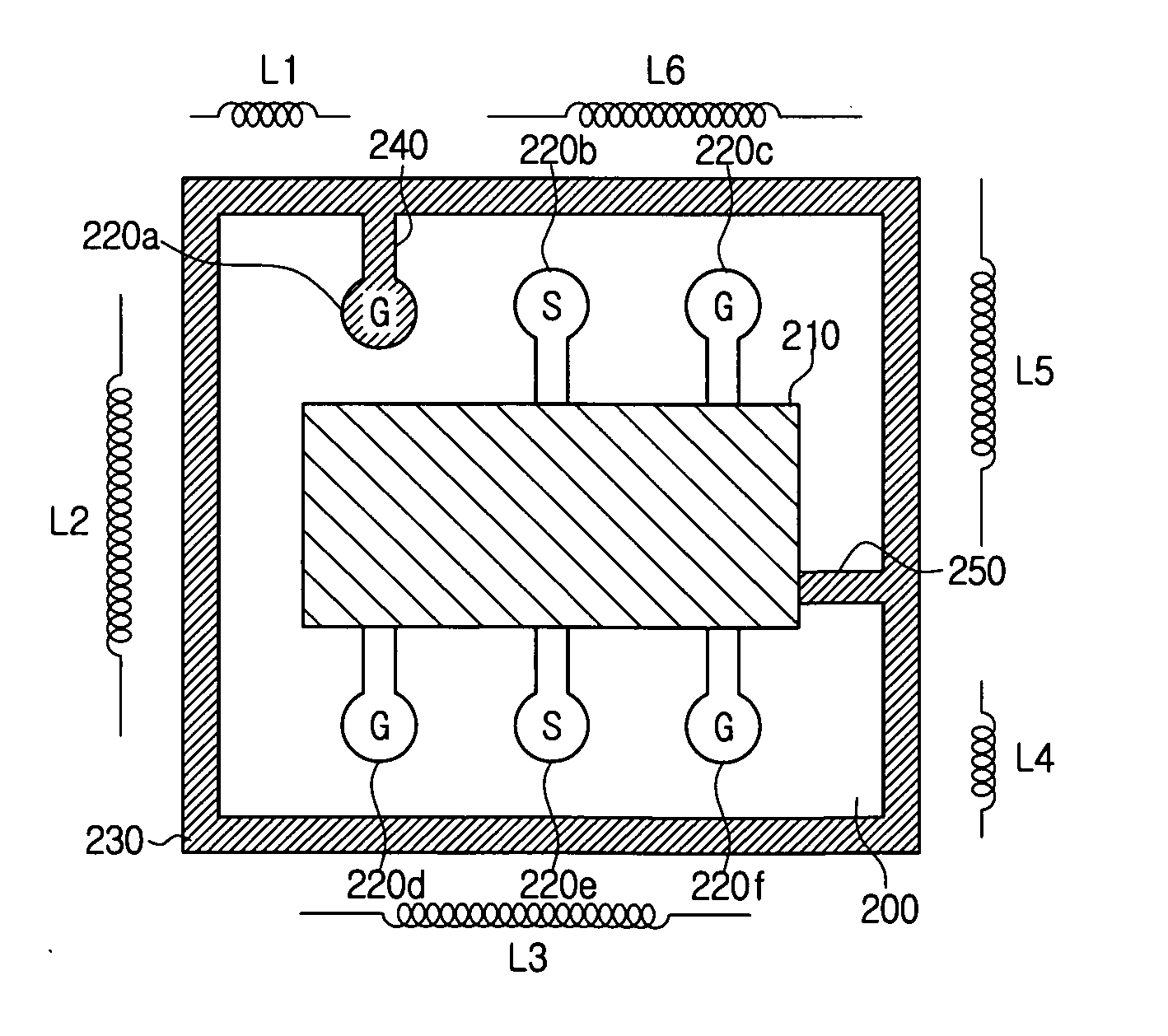
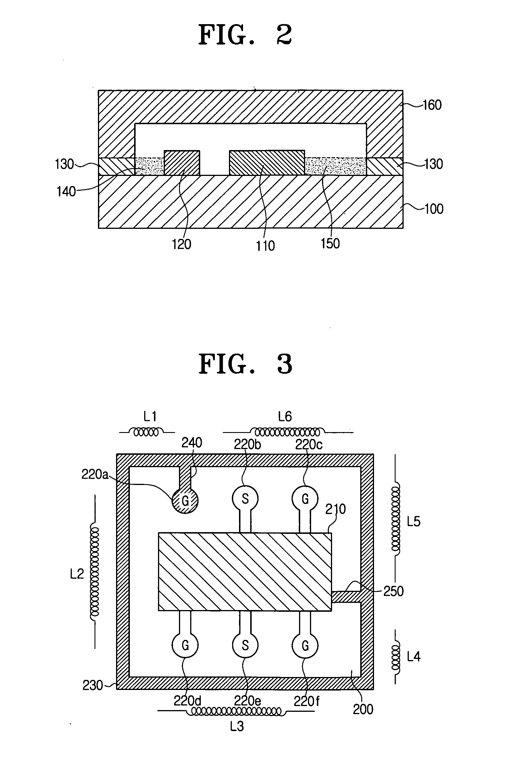
[0022]FIG. 2 is a vertical cross-sectional view for showing a structure of a packaging chip according to an exemplary embodiment of the present invention. In FIG. 2, the packaging chip has a substrate 100, a circuit element 110, a port 120, a sealing line 130, a first connection portion 140, a second connection portion 150, and a packaging substrate 160.

[0023] The substrate 100 can be a general silicon wafer.

[0024] The circuit element 110 can be at least one of various elements such as a resistor, inductor, capacitor, amplifier, bulk acoustic resonator, filter, duplexer, and the like. The circuit element 110 can be mounted on the upper surface of the substrate 100 or built in the substrate 100.

[0025] The port 120 is a portion electrically connected to external terminals. Although not shown in FIG. 2, a via electrode (not shown)...


PUM


Abstract

A packaging chip having inductors therein. The packaging chip includes a substrate for mounting a circuit element therein, at least one port formed on a surface of the substrate, a sealing portion electrically connected on the substrate to the circuit element and the at least one port, respectively, and a packaging substrate bonded to the substrate through the sealing portion and packaging the circuit element. In this case, the sealing portion has a certain magnitude of inductance since it is formed of a conductive material, thereby serving as an inductor. Accordingly, the packaging chip having an inductor therein can be implemented in a small size.

Description

CROSS-REFERENCE TO RELATED APPLICATIONS [0001] This application claims priority under 35 U.S.C. § 119(a) of Korean Patent Application No. 2005-65508, filed Jul. 19, 2005 in the Korean Intellectual Property Office, the entire contents of which are incorporated herein by reference. BACKGROUND OF THE INVENTION [0002] 1. Field of the Invention [0003] The present invention relates to a packaging chip having an inductor therein and, more particularly, to a packaging chip using as an inductor a sealing material needed for packaging. [0004] 2. Description of the Related Art [0005] Electronic chips diversely used in various electronic products can be easily damaged by external shock since the chips have minute electronic circuits therein. Therefore, in the process of manufacturing a chip, a packaging process is inevitably required. [0006] The packaging process refers to a job wherein a circuit element is provided with physical functions and a shape so as to be mounted on an electronic compon...

Claims


Application Information

Patent Timeline
IPC IPC(8): H01L29/00
CPCH01F17/0006H01F27/027H01L2924/16152H01L23/49838H01L23/645H01L23/10H03H3/007
Inventor SIM, DONG-HASONG, IN-SANGKIM, DUCK-HWANPARK, YUN-KWONYUN, SEOK-CHULNAM, KUANG-WOO
Owner SAMSUNG ELECTRONICS CO LTD
Why Eureka
Try Eureka