
Integrated circuit for scan driving

Active Publication Date: 2010-05-11
TEXAS INSTR INC
View PDF9 Cites 0 Cited by
  • Summary
  • Abstract
  • Description
  • Claims
  • Application Information

AI Technical Summary

Benefits of technology

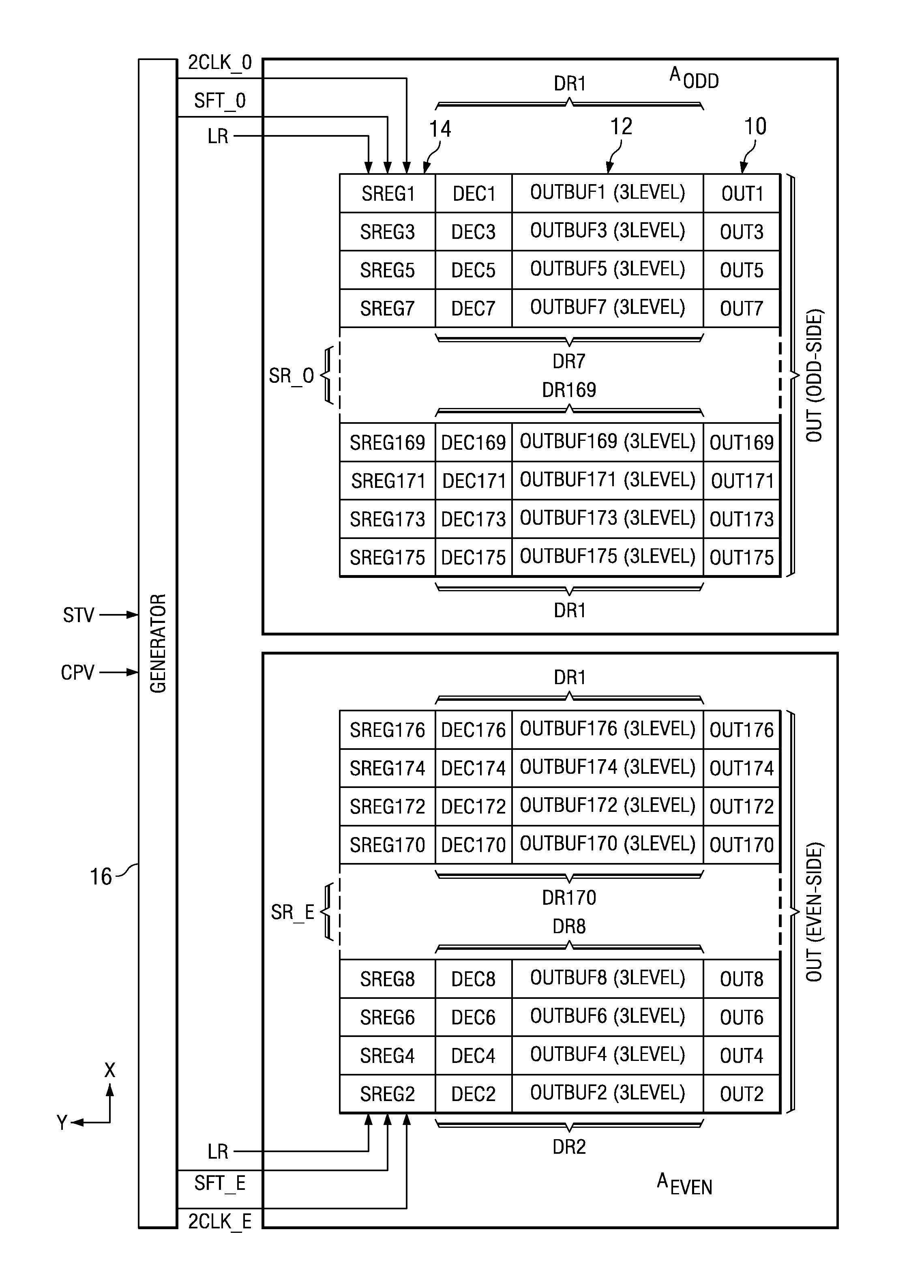
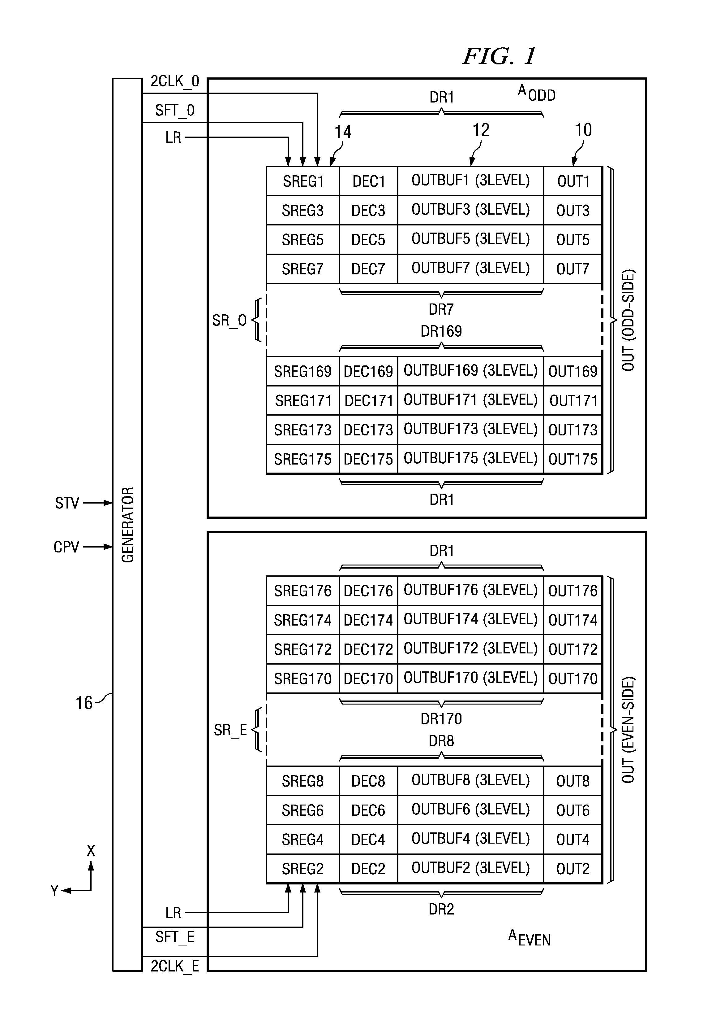
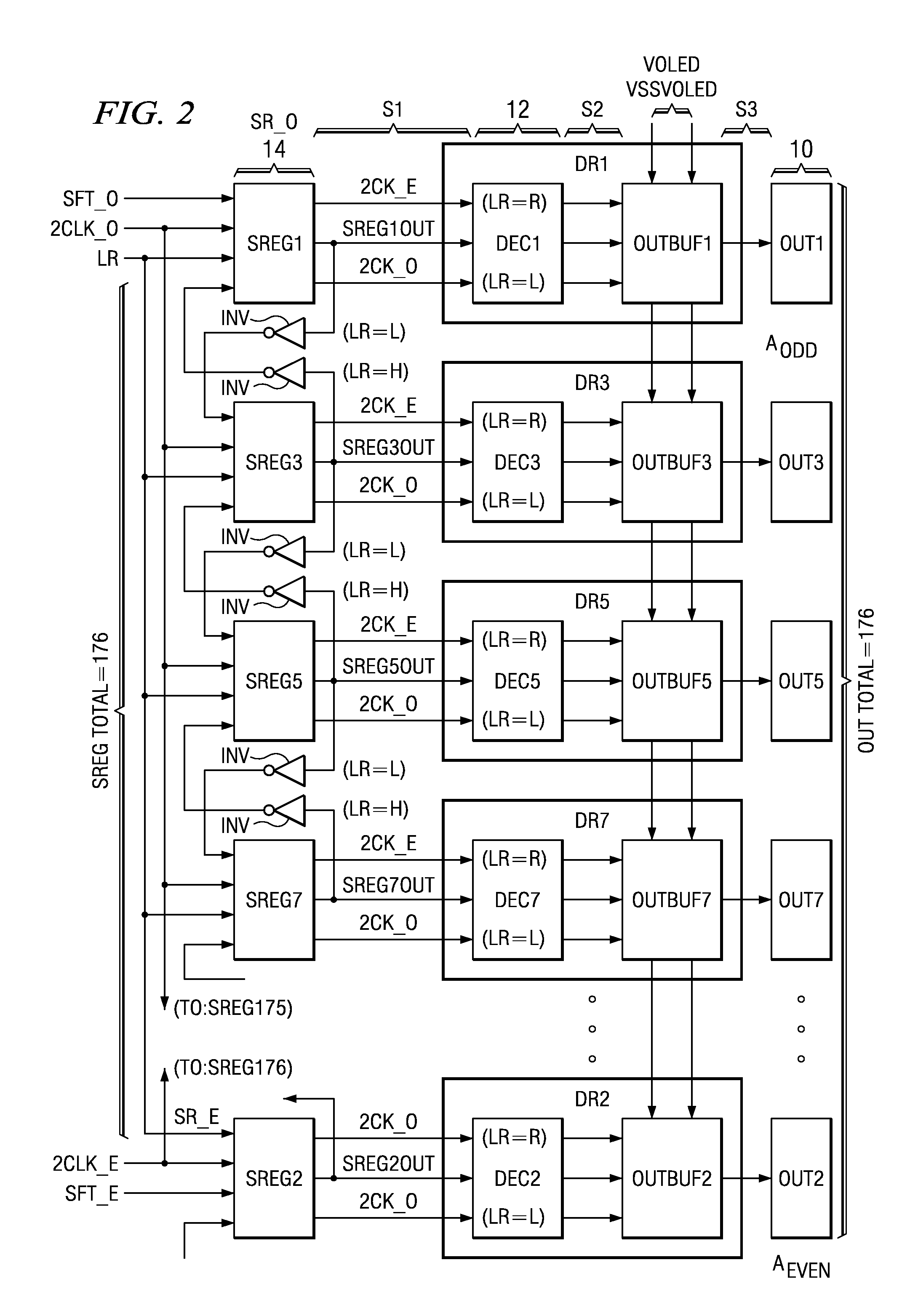
[0033]In the integrated circuit for scan driving, in the first and second regions, driver circuits and selection circuits corresponding to the output pads are arranged in the same row in the second direction. As a result, it is possible to connect the output pads and the driver circuits, as well as the driver circuits and the selection circuits, by wires that extend in the second direction. In the second direction, it is possible to reduce the wiring region size significantly, and it is possible to significantly reduce the chip size.

Problems solved by technology

Also, in TCP, the size in the Y-direction (chip width) may be in the longitudinal direction of the tape, and the increase in the chip size in the longitudinal direction of the tape hampers winding-up of the tape reel (the chip is prone to breakage).
Consequently, it is inappropriate for practical application.

Method used


Image

  • Integrated circuit for scan driving
  • Integrated circuit for scan driving
  • Integrated circuit for scan driving

Examples


Embodiment Construction

[0052]In the following, preferred embodiments of this invention will be explained with reference to FIGS. 1-4.

[0053]The scan driver LSI in this embodiment is mainly characterized by features in the circuit configuration or layout on the chip, while it has the same appearance and external functions of the chip as those in the prior art. Consequently, for the scan driver LSI in this embodiment, one may also adopt the constitution as a slim chip for TCP as shown in FIG. 8, that is, the input terminals or pads VSSOLED, VOLED, Vss, STV, . . . are arranged as a column along one edge in the longitudinal direction of the chip, and, along the opposite edge, output terminals or pads OUT1, OUT3, . . . OUT173, OUT175, OUT176, OUT174, . . . OUT4, OUT2 are arranged as a column. That is, the output pad group is divided into two types, that is, the odd-numbered type OUT1, OUT3, . . . OUT173, OUT175 and the even-numbered type OUT2, OUT4, . . . OUT174, OUT176, and they are [each] arranged as a column...


PUM


Abstract

An integrated circuit is provided for scan driving that can significantly reduce the chip size. In first region AODD, odd-numbered output pads OUT1, OUT3, . . . OUT173, OUT175, driver circuits DR1, DR3, . . . DR173, DR175, and flip-flops SREG1, SREG3, . . . SREG173, SREG175 in an order corresponding to the order of the odd-numbered scanning lines are each arranged as a column in the X-direction, and, at the same time, output pads OUTi, driver circuits DRi and flip-flops SREGi corresponding to the scanning lines are arranged in the same row in the Y-direction (chip width direction). In second region AEVEN, even-numbered output pads OUT2, OUT4, . . . OUT174, OUT176, driver circuits DR2, DR4, . . . DR174, DR176, and flip-flops SREG2, SREG4, . . . SREG174, SREG176 in an order corresponding to the order of the even-numbered scanning lines are each arranged as a column in the X-direction, and, at the same time, output pads OUTi, driver circuits DRi and flip-flops SREGi corresponding to the scanning lines are arranged in the same row in the Y-direction (chip width direction).

Description

RELATED APPLICATION[0001]The present application is based on priority of Japanese Patent Application No. 2002-348991, filed on Nov. 29, 2002.FIELD OF THE INVENTION[0002]The present invention pertains to an integrated circuit (IC or LSI) for scan driving used in flat panel displays, etc. Especially, this invention pertains to a technology for improvement of the circuit configuration on a chip.BACKGROUND OF THE INVENTION[0003]For a liquid crystal display, organic EL display, or other flat panel display, plural scanning lines and plural signal lines are arranged crossing each other in a matrix configuration, and a pixel is arranged at each cross point of the matrix. By means of a scan driver LSI, the scanning lines are selected and driven in a line-sequential scheme. By means of a signal driver LSI, a display signal voltage (image information) is applied or written on each pixel on each selected scanning line so as to display an image.[0004]FIGS. 5-7 illustrate an example of an organic...

Claims


Application Information

Patent Timeline
IPC IPC(8): G09G3/36G02F1/1345G02F1/133G09G3/20G09G3/32G09G5/00H01L51/50H05B33/14
CPCG09G3/20G09G3/3266G09G3/3208G09G2310/08G09G2310/0267G09G2310/0283
Inventor KUBOTA, YASUSHIMURAKAMI, SEIJI
Owner TEXAS INSTR INC
Learn More