
Planar array coil and switching power supply device

a technology of switching power supply and array coil, which is applied in the direction of electric variable regulation, process and machine control, instruments, etc., can solve the problems of failure of power conversion operation of each of the converter circuits that should operate independently, adverse effects of each of the converter circuits on the power conversion operation of each of the converter circuits, and easy unwanted magnetic coupling between the inductors, etc., to achieve stable power conversion operation, and unwanted magnetic coupling between adjacent coil

Pending Publication Date: 2021-04-08
MURATA MFG CO LTD
View PDF0 Cites 0 Cited by
  • Summary
  • Abstract
  • Description
  • Claims
  • Application Information

AI Technical Summary

Benefits of technology

The present patent provides a planar array coil and a switching power supply device that reduce unwanted magnetic coupling between adjacent coils and perform stable power conversion operation. This results in a smaller size of the coil and reduced distance between coils, leading to a more efficient and compact device.

Problems solved by technology

In the case where a plurality of helical inductors are stacked such that winding shafts of the inductors are coincident with each other, as with the inductor array described in Japanese Unexamined Patent Application Publication No. 2015-73052, unwanted magnetic coupling between the inductors easily occurs.
Thus, in a switching power supply device that includes DC-DC converter circuits including inductors, such unwanted magnetic coupling may cause adverse effects on power conversion operation of each of the converter circuits.
That is, failure occurs in power conversion operation of each of the converter circuits that should operate independently.
In such situations, power conversion operation is not performed properly, and power conversion efficiency of the switching power supply device may degrade.

Method used


Image

  • Planar array coil and switching power supply device
  • Planar array coil and switching power supply device
  • Planar array coil and switching power supply device

Examples


first embodiment

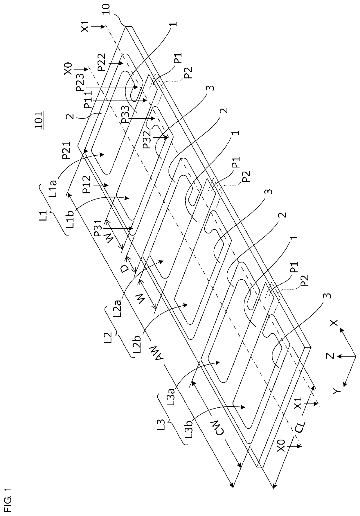
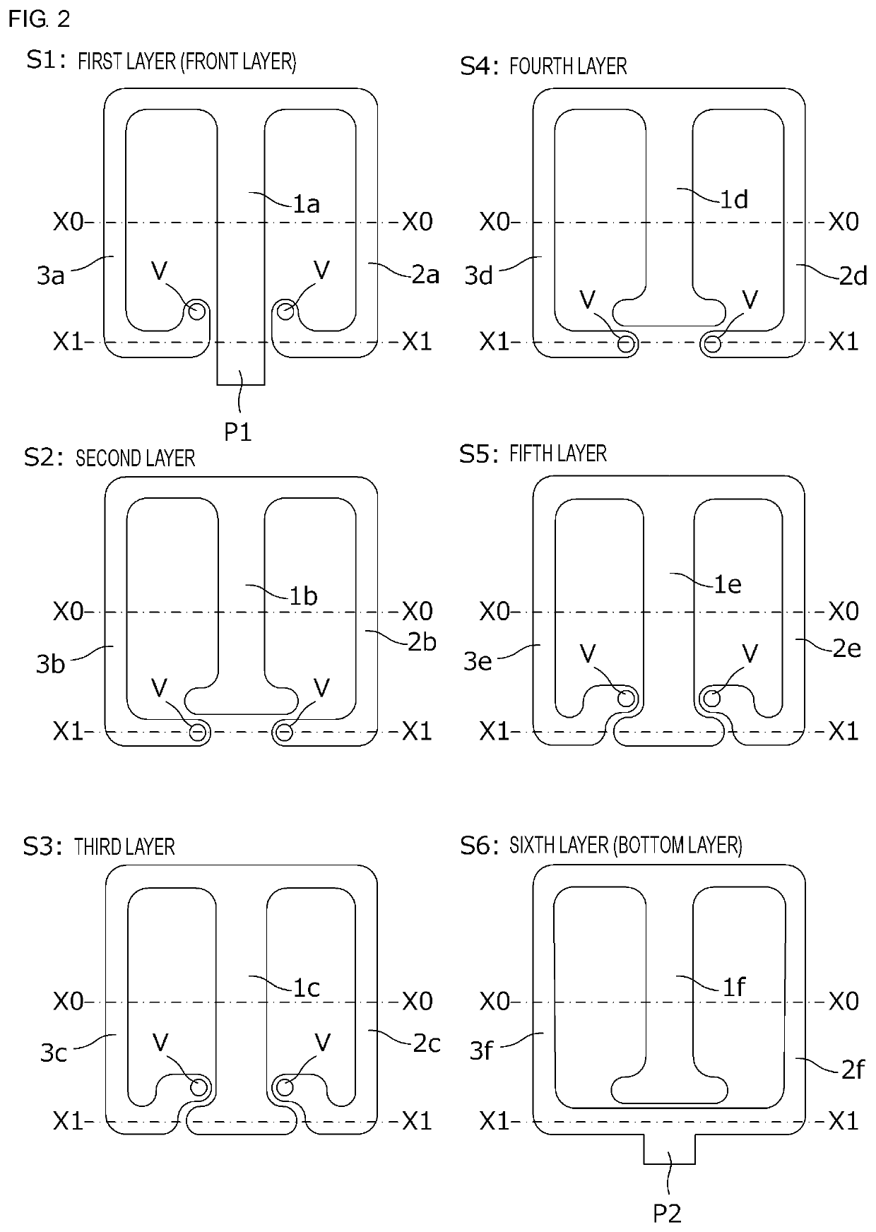
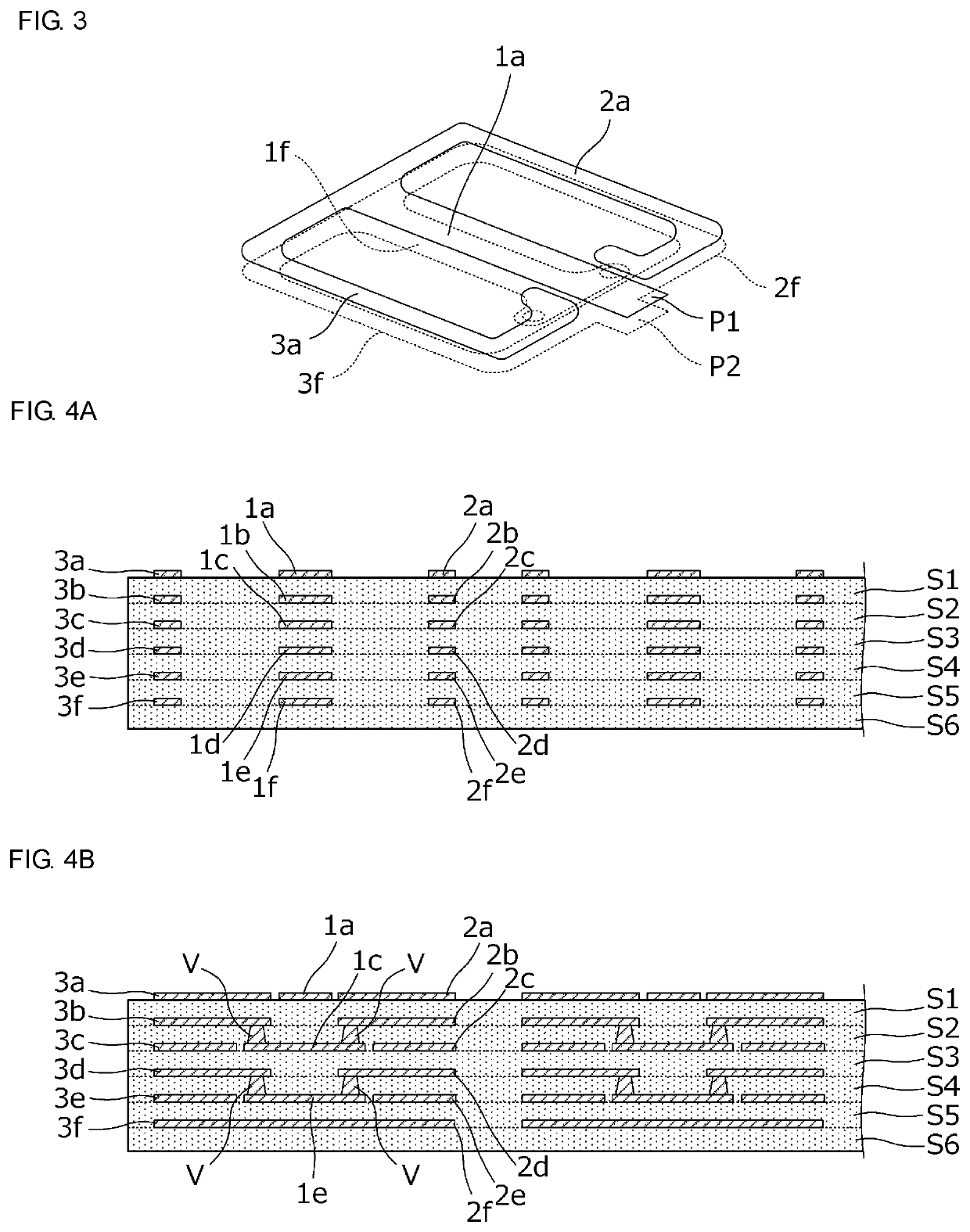
[0035]FIG. 1 is a perspective view of a planar array coil 101 according to a first embodiment. FIG. 2 is an exploded plan view illustrating a structure of a coil of the planar array coil 101 according to this embodiment. FIG. 3 is a perspective view simply illustrating a state in which conductor patterns at individual layers illustrated in FIG. 2 are laminated. FIG. 4A is a longitudinal cross-section view of a part X0-X0 in FIG. 1, and FIG. 4B is a longitudinal cross-section view of a part X1-X1 in FIG. 1. FIG. 5A is a perspective view illustrating current flowing in the planar array coil 101 and generated magnetic flux, and FIG. 5B is a cross-section view of the state illustrated in FIG. 5A.

[0036]The planar array coil 101 according to this embodiment includes a plurality of coils L1, L2, and L3 formed at a multilayer substrate 10. First ends P1 of the coils L1, L2, and L3 are connected to switching circuit units of a power conversion circuit, and second ends P2 of the coils L1, L2,...

second embodiment

[0071]In a second embodiment, some coils having conductor patterns whose shapes are different from those in the first embodiment will be described.

[0072]FIG. 9 is an exploded plan view illustrating a structure of a coil of a planar array coil according to the second embodiment. As in the example illustrated in FIG. 2, only coil conductor patterns formed at individual layers of the multilayer substrate 10 are illustrated in FIG. 9. The coil illustrated in FIG. 9 does not include the fourth layer and the fifth layer illustrated in FIG. 2. That is, one of the coil conductor patterns of the first type formed at the second layer and the fourth layer illustrated in FIG. 2 and one of the coil conductor patterns of the second type formed at the third layer and the fifth layer illustrated in FIG. 2 are provided.

[0073]As described above, the number of laminated conductor patterns may be set in an appropriate manner.

[0074]In FIGS. 2 and 9, the second layer and the third layer form the minimum ...

third embodiment

[0075]In a third embodiment, some coils having conductor patterns whose shapes are different from those in the first embodiment and the second embodiment will be described.

[0076]FIGS. 10, 11, and 12 are exploded plan views illustrating a structure of a coil of a planar array coil according to the third embodiment. As in the examples illustrated in FIGS. 2 and 9, only coil conductor patterns formed at individual layers of a multilayer substrate are illustrated. Bending parts of conductor patterns configuring coils of the planar array coil according to this embodiment do not have a round shape but are bent at right angle, unlike the examples illustrated in FIGS. 2, 9, and so on.

[0077]A coil illustrated in FIG. 10 has a structure in which the second layer and the third layer illustrated in FIG. 9 are removed. That is, the coil has the coil conductor pattern formed at the first layer (front layer) and the coil conductor pattern formed at the second layer (bottom layer) in FIG. 9.

[0078]A...


PUM

PropertyMeasurementUnit
distanceaaaaaaaaaa
frequencyaaaaaaaaaa
self-resonant frequencyaaaaaaaaaa

Abstract

A planar array coil includes a multilayer substrate at which a plurality of coils are formed and arranged on a plane of the multilayer substrate. First ends of the plurality of coils are connected to switching circuit units of a power conversion circuit, and second ends of the plurality of coils are connected to a common output part. The coils include two coil parts in which currents flow in opposite rotation directions, and one coil part of one coil is adjacent to one coil part of another coil. The plurality of coils are connected such that operation of switching circuits causes currents in regions of adjacent coil parts that extend in parallel to each other to flow in the same direction. Accordingly, adverse effects by unwanted coupling between adjacent coils are reduced and a switching power supply device that includes the planar array coil performs stable power conversion operations.

Description

CROSS-REFERENCE TO RELATED APPLICATIONS[0001]This application claims benefit of priority to International Patent Application No. PCT / JP2019 / 007492, filed Feb. 27, 2019, and to Japanese Patent Application No. 2018-153374, filed Aug. 17, 2018, the entire contents of each are incorporated herein by reference.BACKGROUNDTechnical Field[0002]The present disclosure relates to a planar array coil including a plurality of coils arranged on a plane and a switching power supply device including the planar array coil.Background Art[0003]Lamination-type inductor arrays including a plurality of stacked coils have been known, as described, for example, in Japanese Unexamined Patent Application Publication No. 2015-73052. Japanese Unexamined Patent Application Publication No. 2015-73052 discloses an inductor array including a multilayer body in which a plurality of insulation layers and conductor patterns are laminated. The multilayer body includes a first coil and a second coil each including a pl...

Claims


Application Information

Patent Timeline
Patent Type & Authority Applications(United States)
IPC IPC(8): H01F27/28H02M3/155
CPCH01F27/2804H01F41/041H01F2027/2809H02M3/155H01F37/00H02M3/1584H02M3/1586H02M3/003H01F27/346H01F27/366H01F27/255
Inventor HOSOTANI, TATSUYAMIKI, OSAMU
Owner MURATA MFG CO LTD
Learn More