
Composite electronic component

a technology of electronic components and composites, applied in the direction of cross-talk/noise/interference reduction, association of printed circuit non-printed electric components, printed element electric connection formation, etc., can solve the problem of difficult and achieve the effect of miniaturization of composite electronic components and suppressing unwanted coupling within multi-layer wiring boards

Inactive Publication Date: 2006-11-02
PANASONIC CORP
View PDF7 Cites 0 Cited by
  • Summary
  • Abstract
  • Description
  • Claims
  • Application Information

AI Technical Summary

Benefits of technology

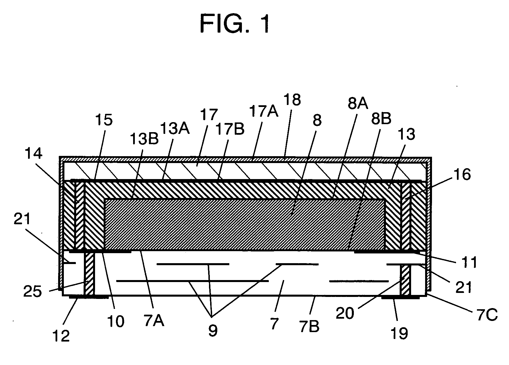
[0006] A composite electronic component of the present invention has a multi-layer wiring board, a first power terminal electrode, a second power terminal electrode, an external connection power supply terminal, a surface-mounted component, an insulator, and a power supply pattern. The first power terminal electrode and the second power terminal electrode are disposed on a first face of the multi-layer wiring board. The external connection power supply terminal is disposed on a second face opposite to the first face of the multi-layer wiring board and connected with the first power terminal electrode. The surface-mounted component is mounted on the first face of the multi-layer wiring board and connected with the first power terminal electrode and the second power terminal electrode at a first face of the surface-mounted component. The insulator covers at least a second face opposite to the first face of the surface-mounted component, as well as the first power terminal electrode and the second power terminal electrode with a first face of the insulator. The power supply pattern is disposed on a second face opposite to the first face of the insulator and connected with the first power terminal electrode and the second power terminal electrode. According to the configuration described above, the power supply pattern as a power supply path branched from a path connecting the external connection power supply terminal with the first power terminal electrode comes to be located outside the multi-layer wiring board. Therefore, unwanted coupling within the multi-layer wiring board can be suppressed and thus miniaturization of the composite electronic component can be attained.

Problems solved by technology

However, routed portion 5 of the power supply path within board 1 becomes a cause of unnecessary coupling with other circuit electrodes 6 disposed within board 1 in a high-frequency range.
Thus, it is necessary to increase inter-electrode distances and this makes it difficult to miniaturize the composite electronic component.

Method used


Image

  • Composite electronic component
  • Composite electronic component
  • Composite electronic component

Examples


Embodiment Construction

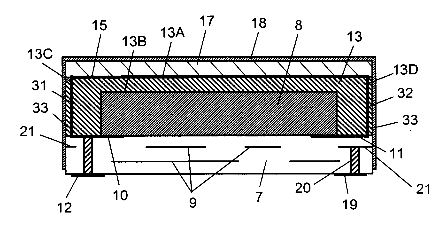
[0051]FIG. 1 is a schematic sectional view schematically showing a configuration of a composite electronic component having a surface-mounted component mounted on a multi-layer wiring board, according to an embodiment of the present invention. Multi-layer wiring board (hereinafter called “board”) 7 is formed by laminating insulating layers of resin. Between the layers, there are disposed circuit electrodes (hereinafter called “electrode”) 9 for forming a high-frequency circuit with use of capacitors, inductors, and the like. On upper face 7A as a first face of board 7, there are disposed first and second power terminal electrodes (hereinafter called “electrodes”) 10, 11, while on lower face7B as a second face opposite to the first face, there is disposed external connection power supply terminal (hereinafter called “terminal”) 12. Electrode 10 and terminal 12 are connected by way of via 25. Surface-mounted component (hereinafter called “component”) 8 is controlled for its operation ...


PUM


Abstract

A composite electronic component having a multi-layer wiring board, a first power terminal electrode, a second power terminal electrode, an external connection power supply terminal, a surface-mounted component, an insulator, and a power supply pattern. The first and the second power terminal electrodes are disposed on a first face of the multi-layer wiring board. The external connection power supply terminal is disposed on a second face opposite to the first face of the multi-layer wiring board and connected with the first power terminal electrode. The surface-mounted component is mounted on the first face of the multi-layer wiring board and connected with the first and the second power terminal electrodes at a first face thereof. The insulator covers at least a second face opposite to the first face of the surface-mounted component, the first power terminal electrode, and the second power terminal electrode with a first face thereof. The power supply pattern is disposed on a second face opposite to the first face of the insulator and connected with the first and the second power terminal electrodes.

Description

[0001] This application is a U.S. National Phase Application of PCT International Application PCT / JP2005 / 008140, filed Apr. 28, 2005. TECHNICAL FIELD [0002] The present invention relates to a composite electronic component provided by mounting a surface-mounted component on a multi-layer wiring board. BACKGROUND ART [0003]FIG. 4 is a sectional view schematically showing a conventional composite electronic component. The composite electronic component has surface-mounted component (hereinafter called “component”) 3, such as a semiconductor device requiring a control voltage, mounted on multi-layer wiring board (hereinafter called “board”) 1. On the surface of board 1, there are disposed power terminal electrodes (hereinafter called “electrodes”) 2, and component 3 is mounted so as to be connected with electrodes 2. [0004] In some of such composite electronic components, a plurality of control voltages for synchronous control are applied to component 3. In such a case, the control of ...

Claims


Application Information

Patent Timeline
Patent Type & Authority Applications(United States)
IPC IPC(8): H01L23/12H05K3/46H01L23/00H01L23/28H05K1/02H05K1/18H05K3/00H05K3/40
CPCH01L24/97H01L2924/12041H01L2924/01047H01L2924/01056H01L2924/01074H01L2924/01082H01L2924/19041H01L2924/19042H01L2924/19043H01L2924/30105H01L2924/30107H01L2924/3025H05K1/0218H05K1/0263H05K1/167H05K1/186H05K3/0052H05K3/403H05K3/4614H05K2201/0715H05K2203/061H01L2924/01006H01L2924/01033
Inventor TSUNEOKA, MICHIAKISUGAYA, YASUHIROKATSUMATA, MASAAKIFUJIWARA, JOJI
Owner PANASONIC CORP
Learn More