
Illumination apparatus comprising passive optical nanostructures

a technology of passive optical nanostructures and illumination apparatuses, which is applied in the direction of electrical apparatus, nanotechnology, semiconductor devices, etc., can solve the problems of difficult manufacturing of appropriate passive optical structures, and achieve the effects of low cost, high efficiency and low cos

Active Publication Date: 2021-04-08
REALD SPARK LLC
View PDF1 Cites 3 Cited by
  • Summary
  • Abstract
  • Description
  • Claims
  • Application Information

AI Technical Summary

Benefits of technology

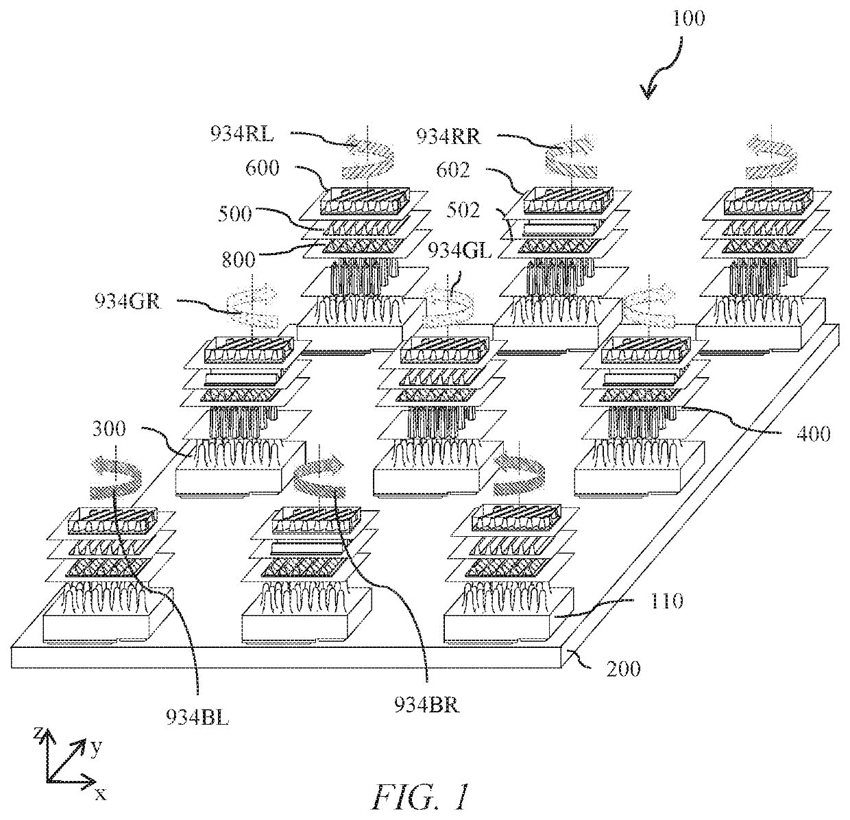
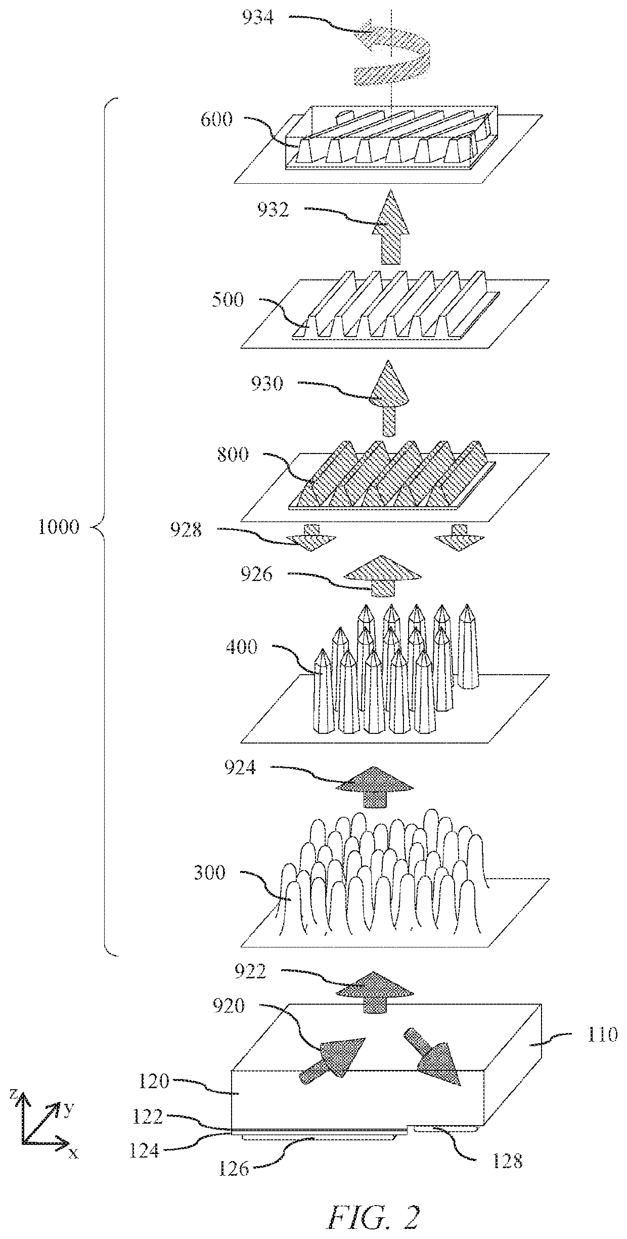
This patent describes a way to have thin layers of light emitting elements that produce high quality light output. The layers can be aligned using a special nanostructure, which allows for many layers to be aligned simultaneously, reducing cost and complexity. The resulting display apparatus is very thin and can have high quality optical output at a low cost.

Problems solved by technology

It tends to be difficult to manufacture appropriate passive optical structures which work well with light-emitting elements having the size of micro-LEDs.

Method used


Image

  • Illumination apparatus comprising passive optical nanostructures
  • Illumination apparatus comprising passive optical nanostructures
  • Illumination apparatus comprising passive optical nanostructures

Examples


Embodiment Construction

[0075]In this specification, (except when qualified by the term “packaged”), “LED” or “micro-LED” refers to an unpackaged LED die chip extracted directly from a monolithic wafer, i.e. a semiconductor element. Micro-LEDs may be formed by array extraction methods in which multiple LEDs are removed from a monolithic epitaxial wafer in parallel and may be arranged with positional tolerances that are less than 5 micrometres. This is different from packaged LEDs. Packaged LEDs typically have a lead-frame and plastic or ceramic package with solder terminals suitable for standard surface-mount PCB (printed circuit board) assembly. The size of the packaged LEDs and limits of PCB assembly techniques means that displays formed from packaged LEDs are difficult to assemble with pixel pitches below about 1 mm. The accuracy of components placed by such assembly machines is typically about plus or minus 30 micrometres. Such sizes and tolerances prevent application to very high-resolution displays.

[...


PUM

PropertyMeasurementUnit
sizeaaaaaaaaaa
widthaaaaaaaaaa
widthaaaaaaaaaa

Abstract

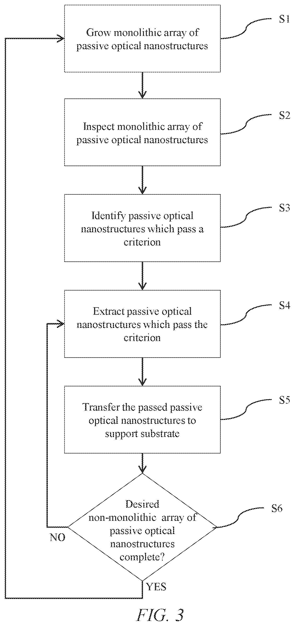
An illumination apparatus is manufactured by selectively removing passive optical nanostructures from a monolithic array of light-emitting elements while preserving their relative spatial position. The nanostructures are selected such that, in at least one direction, for at least one pair of the selectively removed passive optical nanostructures, for each respective pair there is at least one nanostructure that is not selected that was positioned in the monolithic array between the pair of selectively removed passive optical nanostructures in the at least one direction, forming a non-monolithic array of passive optical nanostructures with the selectively removed passive optical nanostructures while preserving their relative spatial position, and aligning each of the passive optical nanostructures of the non-monolithic array with a respective light-emitting element of the non-monolithic array of light-emitting elements.

Description

TECHNICAL FIELD[0001]This disclosure generally relates to modification of optical output from illumination devices and methods to manufacture illumination apparatuses including display apparatuses comprising passive optical nanostructures. Said illumination apparatuses may be used in applications such as environmental illumination or for image display.BACKGROUND[0002]In illumination apparatuses, passive optical structures (e.g. polarising elements, colour conversion elements etc.) are often incorporated to control the way the illumination apparatus provides light. One type of illumination apparatus is an illumination apparatus which uses micro-LEDs as the light-emitting elements. It tends to be difficult to manufacture appropriate passive optical structures which work well with light-emitting elements having the size of micro-LEDs.BRIEF SUMMARY[0003]According to the present disclosure, there is provided a method for manufacturing an illumination apparatus, the method comprising: for...

Claims


Application Information

Patent Timeline
Patent Type & Authority Applications(United States)
IPC IPC(8): H01L33/58B82Y20/00H01L33/24H01L33/62
CPCH01L33/58B82Y20/00H01L2933/0058H01L33/62H01L33/24H01L25/0753H01L33/505H01L33/502H01L33/60B82Y40/00
Inventor HARROLD, JONATHANROBINSON, MICHAEL G.WOODGATE, GRAHAM J.
Owner REALD SPARK LLC
Learn More