Display device, organic electroluminescence display device and manufacturing method thereof

a display device and organic technology, applied in semiconductor devices, solid-state devices, diodes, etc., can solve problems such as affecting product yield, and achieve the effects of avoiding color mixed illumination, effective preventing the hole from passing, and improving product yield

Active Publication Date: 2021-06-17
WUHAN CHINA STAR OPTOELECTRONICS SEMICON DISPLAY TECH CO LTD
View PDF0 Cites 0 Cited by
  • Summary
  • Abstract
  • Description
  • Claims
  • Application Information

AI Technical Summary

Benefits of technology

[0042]In the present application, the hole blocking layer includes the first hole blocking region, the second hole blocking region, and the third hole blocking region that are disposed at different positions. The first hole blocking region is disposed at a position corresponding to the first light emitting region of the light emitting layer, the second hole blocking region is disposed at a position corresponding to the second light emitting region of the light emitting layer, and the third hole blocking region is disposed at a position corresponding to the third light emitting region of the light emitting layer. When the ligh...

Problems solved by technology

It is easy for this process to cause misalignment.
The organic electroluminescence display...

Method used


Image

  • Display device, organic electroluminescence display device and manufacturing method thereof
  • Display device, organic electroluminescence display device and manufacturing method thereof
  • Display device, organic electroluminescence display device and manufacturing method thereof

Examples


Embodiment Construction

[0048]To make the objectives, technical schemes, and effects of the present application more clear and specific, the present application is described in further detail below with reference to the embodiments in accompanying with the appending drawings. It should be understood that the specific embodiments described herein are merely for explaining the present application, the term “embodiment” used in the context means an example, instance, or illustration, and the present application is not limited thereto.

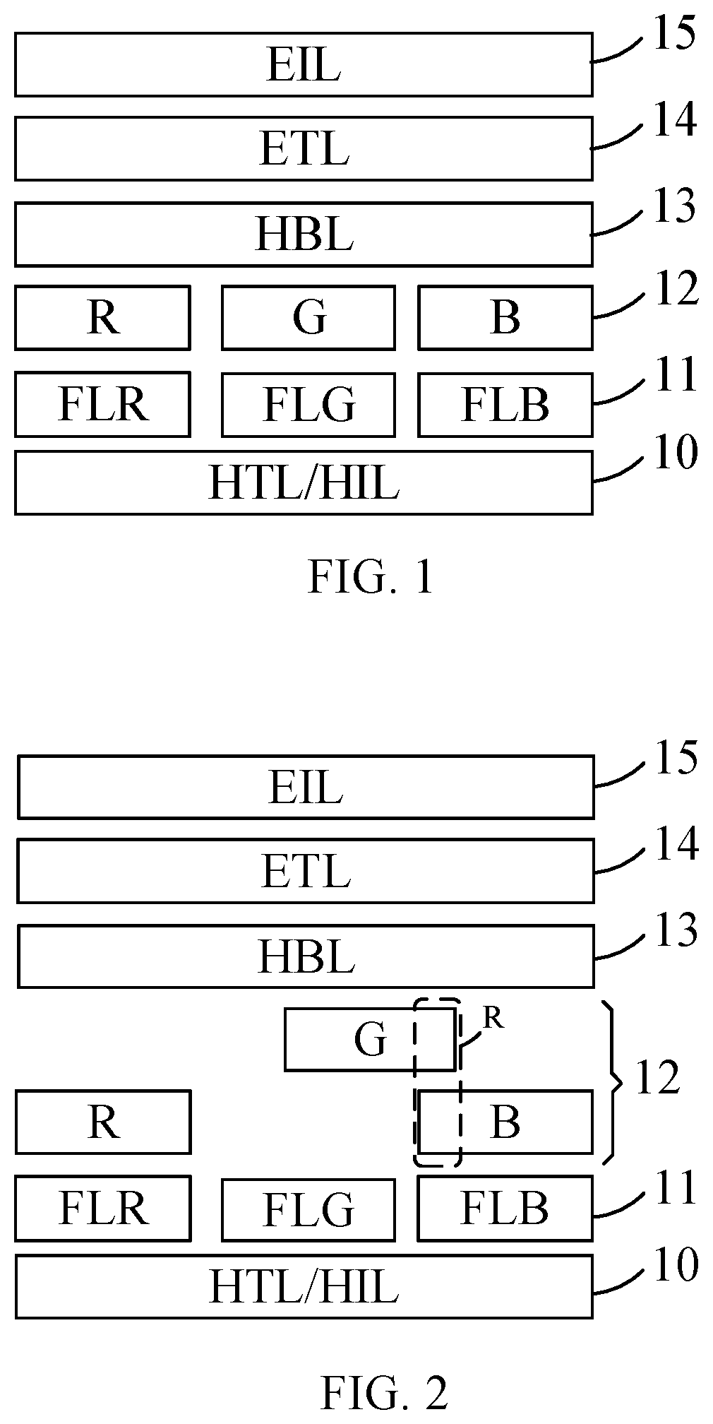
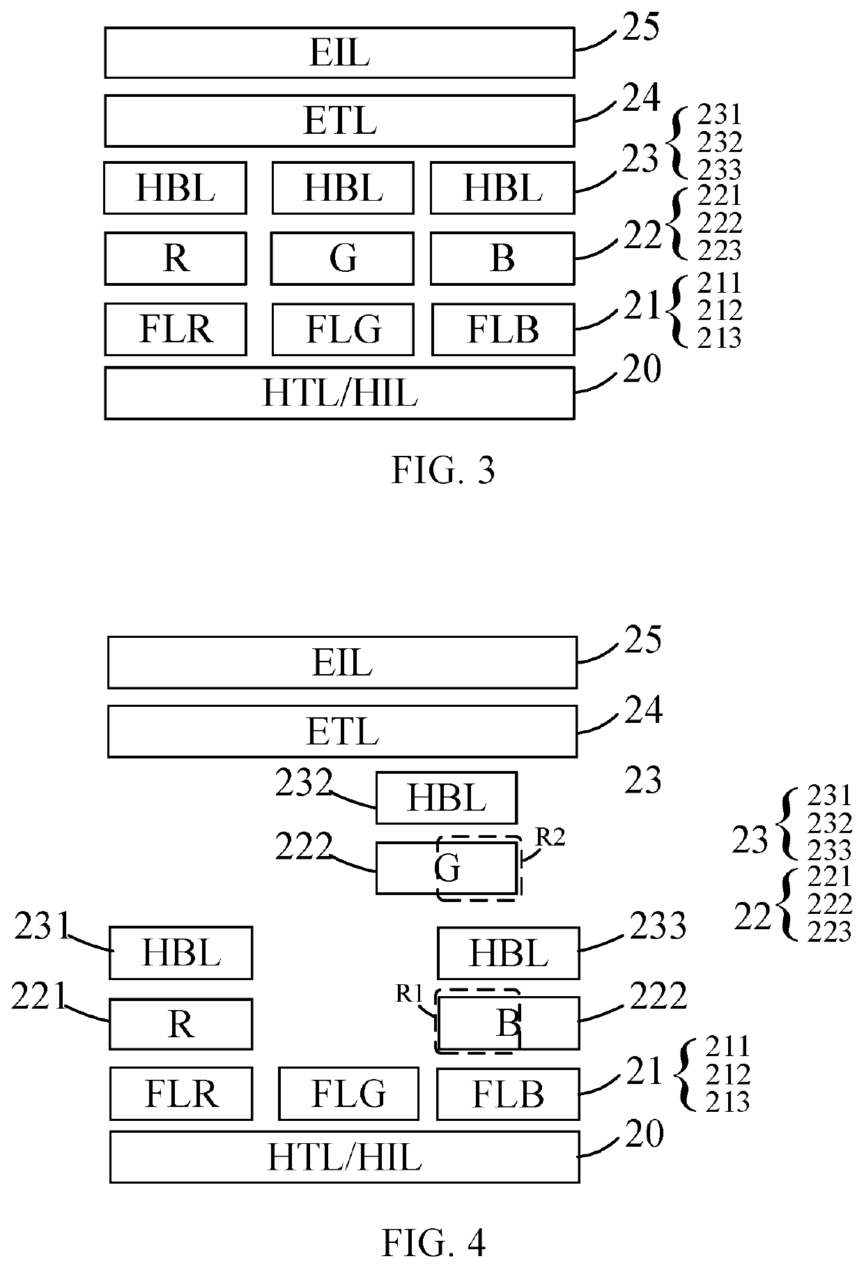
[0049]FIG. 3 is a schematic diagram showing an organic electroluminescence display device according to the present application. As shown in FIG. 3, the organic electroluminescence (EL) display device includes a hole transport functional layer 20, a fluorescent material layer 21, a light emitting layer 22, a hole blocking layer (HBL) 23, and an electron transport functional layer (including an electron transport layer (ETL) 24 and an electron injection layer (EIL) 25). The organic...


PUM


Abstract

A display apparatus, and an organic electroluminescence display device and a manufacturing method thereof are provided. The organic electroluminescence display device includes a hole transport functional layer; a light emitting layer disposed on the hole transport functional layer, which includes a first, a second, and a third light emitting regions that emit light rays of different colors; a hole blocking layer disposed on the light emitting layer, which includes a first, a second, and a third hole blocking regions that are disposed at different positions, the first, the second, and the third hole blocking layers disposed at positions corresponding to the first, the second, and the third light emitting regions, respectively; and an electron transport functional layer disposed on the hole blocking layer. The present application solves a technical problem of color mixing for light rays emitted from the light emitting layer and improves product yield.

Description

FIELD OF THE DISCLOSURE[0001]The present application relates to display technologies, and more particularly to a display device, and an organic electroluminescence display device and a manufacturing method thereof.DESCRIPTION OF RELATED ARTS[0002]In an organic light emitting diode (OLED) display apparatus, every one of pixel structures includes a plurality of subpixels and each of the subpixels includes an organic electroluminescence (EL) display device including an anode, a cathode, and a light emitting layer disposed between the anode and the cathode. The light emitting layer is driven by an electric field between the anode and the cathode and emits light rays by injection and recombination of charge carriers. The light emitting layer can produce light rays of different colors when manufactured using different materials.[0003]FIG. 1 is a schematic diagram showing an organic electroluminescence display device in an existing art. As shown in FIG. 1, the organic electroluminescence d...

Claims


Application Information

Patent Timeline
IPC IPC(8): H01L51/50H01L51/56
CPCH01L51/5056H01L27/3209H01L51/5096H01L51/56H10K59/32H10K50/131H10K50/18H10K50/11H10K2101/10H10K71/00H10K59/35H10K50/15
Inventor PEI, LONG
Owner WUHAN CHINA STAR OPTOELECTRONICS SEMICON DISPLAY TECH CO LTD
Why Eureka
Try Eureka