Check patentability & draft patents in minutes with Patsnap Eureka AI!

MIM capacitor of embedded structure and method for making the same

a technology of embedded structure and capacitor, which is applied in the direction of capacitors, semiconductor devices, semiconductor/solid-state device details, etc., can solve the problems of adverse effects on the performance and reliability of mim capacitors, and it is difficult to control the amount of over-etching, so as to avoid adverse effects and improve performance and reliability of capacitors.

Active Publication Date: 2021-07-01
HUA HONG SEMICON WUXI LTD
View PDF0 Cites 0 Cited by
  • Summary
  • Abstract
  • Description
  • Claims
  • Application Information

AI Technical Summary

Benefits of technology

The present patent text describes an improved method for manufacturing an embedded MIM capacitor to improve its performance and reliability. The method involves connecting the capacitor lower electrode to the bottom metal wire layer through a via, while the capacitor upper electrode is directly in contact with the top metal wire layer. Additionally, a side wall is formed on the side face of the MIM capacitor to isolate it from the second metal wire layer. This structure avoids the adverse impact of vias on the MIM capacitor, resulting in improved performance and reliability.

Problems solved by technology

Therefore, the via 105a usually undergoes over-etching, and it is not easy to control the amount of over-etching, finally imposing adverse impacts on the performance and reliability of the MIM capacitor.

Method used


Image

  • MIM capacitor of embedded structure and method for making the same
  • MIM capacitor of embedded structure and method for making the same
  • MIM capacitor of embedded structure and method for making the same

Examples


Embodiment Construction

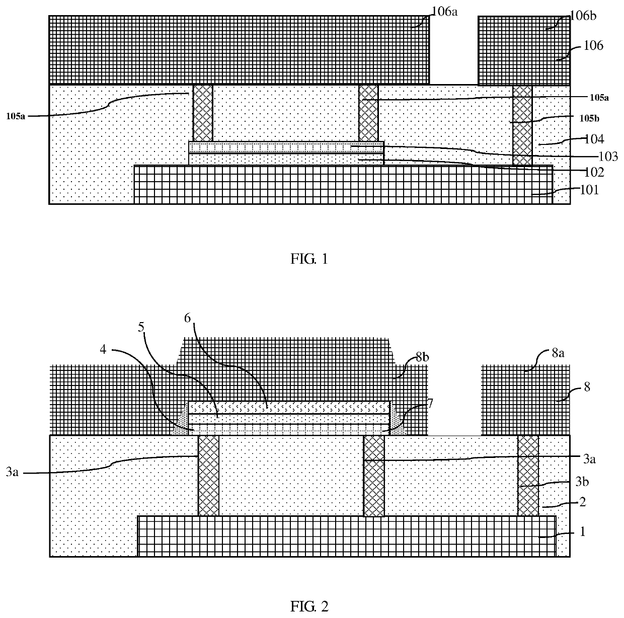
[0054]Referring to FIG. 2, which is a structural schematic view of an MIM capacitor of an embedded structure in an embodiment of the present application, it can be seen that the MIM capacitor of an embedded structure in the embodiment of the present application is formed between a first metal wire layer 1 and a second metal wire layer 8 arranged in an upper-lower adjacent manner.

[0055]An interlayer film 2 is formed between the first metal wire layer 1 and the second metal wire layer 8.

[0056]Generally, the first metal wire layer 1 is formed on a semiconductor substrate. The semiconductor substrate includes a silicon substrate, a semiconductor device is formed in the semiconductor substrate, more than one layer of bottom interlayer film is formed in the semiconductor substrate before the first front metal layer is formed, and a corresponding bottom front metal layer is formed between the bottom interlayer films.

[0057]The MIM capacitor is formed on the surface of the interlayer film 2 ...


PUM


Abstract

The present application has disclosed an MIM capacitor of an embedded structure, wherein an interlayer film is formed between a first metal wire layer and a second metal wire layer; the MIM capacitor is formed on the surface of the interlayer film; a capacitor lower electrode is connected to the first metal wire layer by means of a bottom first via, the first metal wire layer is connected, by means of a second via outside the capacitor lower electrode, to a lower electrode lead-out structure formed by the second metal wire layer; and an upper electrode lead-out structure formed by the second metal wire layer covers the surface of the capacitor upper electrode of the MIM capacitor. The present application has further disclosed a method for manufacturing an MIM capacitor of an embedded structure. In the present application, the performance and stability of the capacitor can be improved.

Description

CROSS-REFERENCES TO RELATED APPLICATIONS[0001]This application claims priority to Chinese patent application number 201911363247.9 filed at CNIPA on Dec. 26, 2019, and entitled “MIM CAPACITOR OF EMBEDDED STRUCTURE AND METHOD FOR MAKING THE SAME”, the disclosure of which is incorporated by reference herein its entirely.TECHNICAL FIELD[0002]The present application relates to the field of semiconductor integrated circuit manufacturing, in particular to an MIM capacitor of an embedded structure; and the present application further relates to a method for manufacturing an MIM capacitor of an embedded structure.BACKGROUND[0003]Referring to FIG. 1, which is a structural schematic view of an existing MIM capacitor of an embedded structure, it can be seen that the existing MIM capacitor of an embedded structure is formed between a first metal wire layer 101 and a second metal wire layer 106 arranged in the upper-lower adjacent manner.[0004]The first metal wire layer 101 directly serves as a ...

Claims


Application Information

Patent Timeline
IPC IPC(8): H01L23/522H01L49/02H01L21/768
CPCH01L23/5223H01L21/76877H01L28/60H01L23/5222H01L21/768
Inventor CHEN, YU
Owner HUA HONG SEMICON WUXI LTD
Features
  • R&D
  • Intellectual Property
  • Life Sciences
  • Materials
  • Tech Scout
  • Unparalleled Data Quality
  • Higher Quality Content
  • 60% Fewer Hallucinations
Learn More