

Light emitting display device
- Summary
- Abstract
- Description
- Claims
- Application Information
AI Technical Summary
Benefits of technology
Problems solved by technology
Method used
Image

Examples
first embodiment
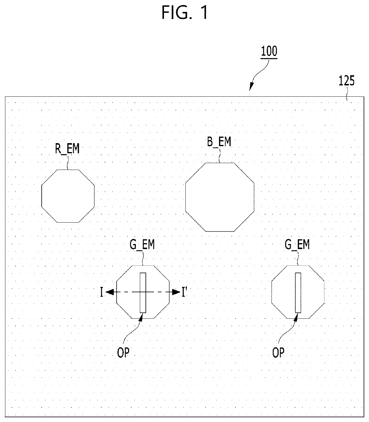
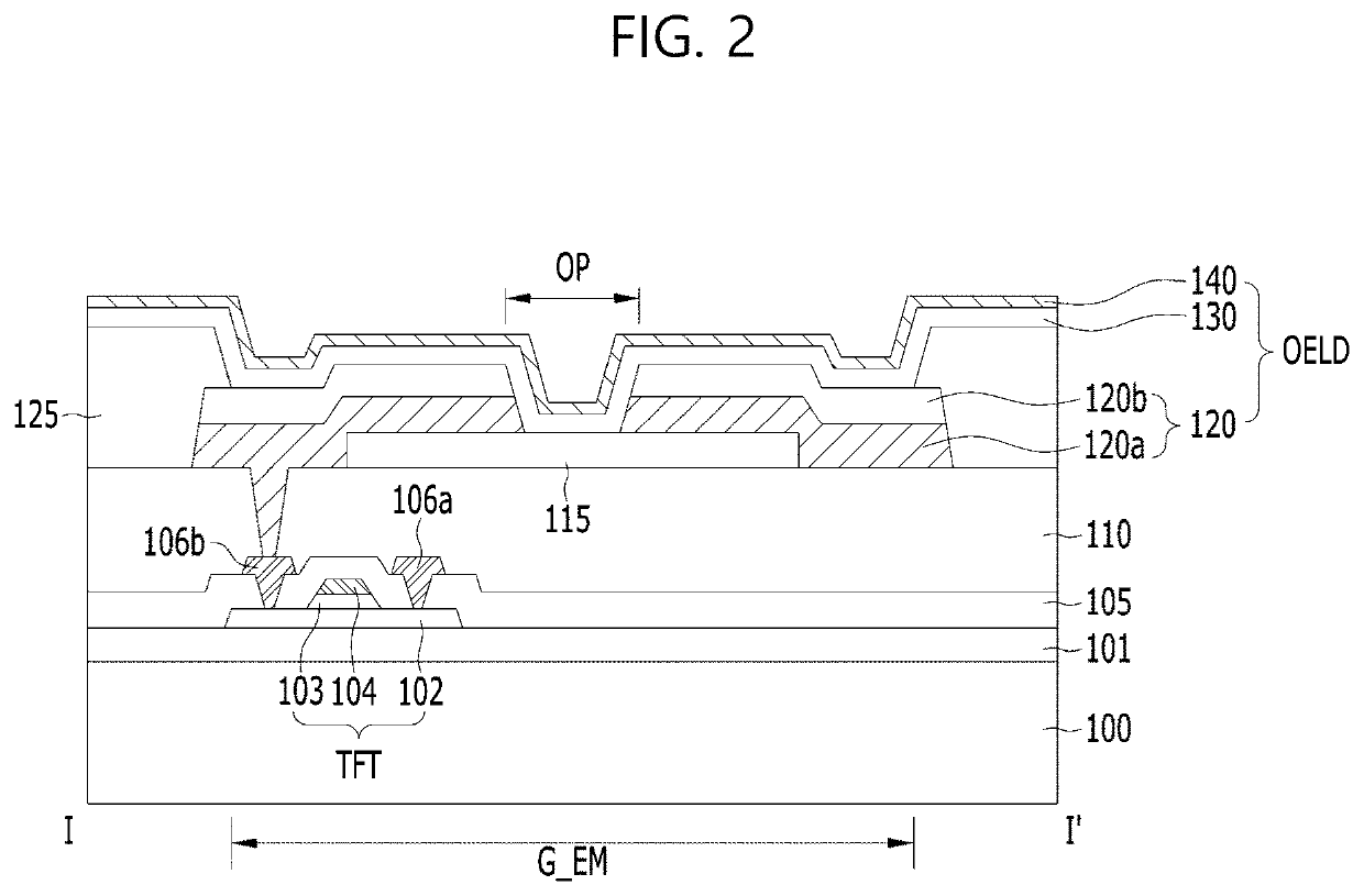
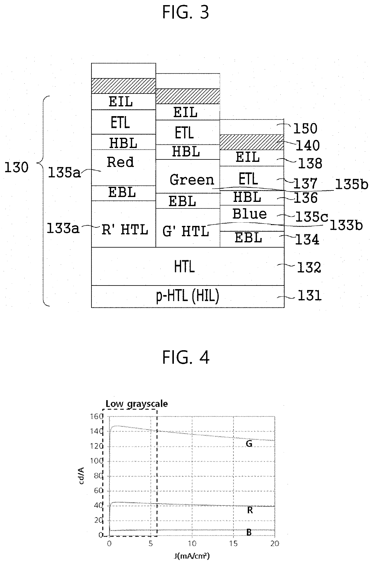
[0034]FIG. 1 is a plan view illustrating a light emitting display device according to the present invention, and FIG. 2 is a cross-sectional view taken along line I-I′ of FIG. 1. FIG. 3 is a cross-sectional view illustrating light emitting elements in a red light emitting part, a green light emitting part and a blue light emitting part of the light emitting display device of FIG. 1.
[0035]As shown in FIGS. 1 and 2, the light emitting display device according to the present invention includes first light emitting parts R_EM, second light emitting parts G_EM and third light emitting parts B_EM which emit light of different colors, on a substrate 100.
[0036]A bank 125 is configured to be provided between the first to third light emitting parts R_EM, G_EM and B_EM, and the respective first to third light emitting parts R_EM, G_EM and B_EM are exposed through open areas of the bank 125. Here, a subpixel SP means an area including each light emitting part R_EM, G_EM or B_EM and a region of ...
second embodiment
[0078]As shown in FIG. 5A, in the light emitting display device according to the present invention, openings OP1-OP5 formed in an anode 220 of a light emitting part EM may be a plurality of linear-shaped slits which are spaced apart from each other by the same interval. The openings OP1-OP5 may be formed by selectively removing the anode 220. In order to exhibit current spreading effects in the anode 220 having the openings OP1-OP5, portions of the anode 220 located at the edges of the openings OP1-OP5 are connected.
third embodiment
[0079]As shown in FIG. 5B, in the light emitting display device according to the present invention, an opening OP formed in an anode 320 may be formed in a cross shape in which a first opening part OP1 formed in a vertical direction and a second opening part OP2 formed in a horizontal direction are connected.
[0080]In this case, in order to exhibit current spreading effects in the anode 320, portions of the anode 320 located around the opening OP are connected.
PUM
 Abstract
Description
Claims
Application Information