Sensor chip and distance measurement device

Pending Publication Date: 2022-06-09
SONY SEMICON SOLUTIONS CORP
View PDF0 Cites 0 Cited by
  • Summary
  • Abstract
  • Description
  • Claims
  • Application Information

AI Technical Summary

Benefits of technology

The patent is about a sensor chip and a distance measurement device that can make pixels smaller. The technical effect is to improve the accuracy and resolution of the sensor.

Problems solved by technology

In a distance measurement image sensor (a distance measurement device) that uses a single photon avalanche diode (SPAD), light emission in a high electric field region in a pixel at the time of multiplication of carriers can cause a photon to enter an adjacent pixel, thereby causing a signal to be unintentionally detected in the adjacent pixel.

Method used


Image

  • Sensor chip and distance measurement device
  • Sensor chip and distance measurement device
  • Sensor chip and distance measurement device

Examples


embodiment

1. Embodiment

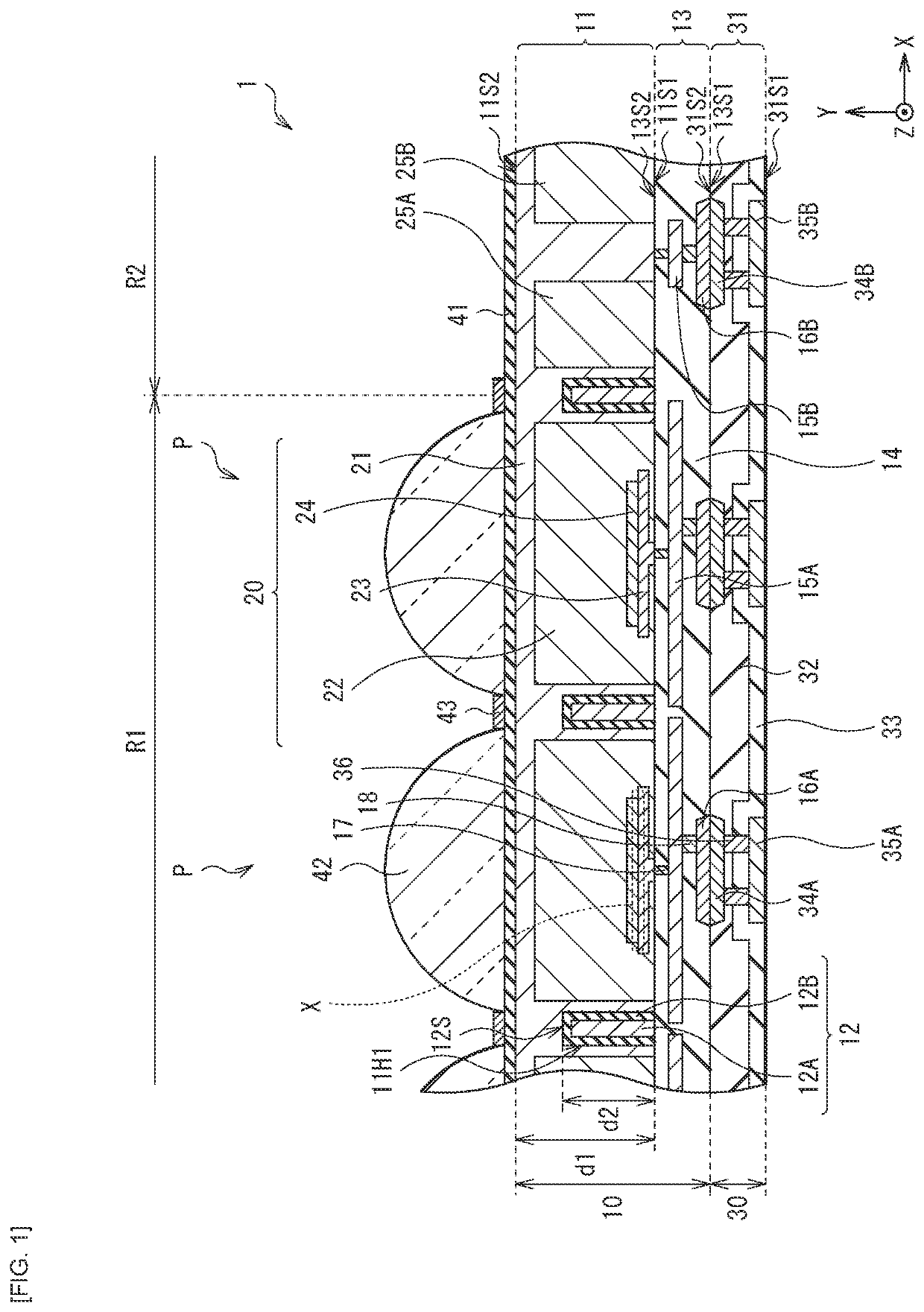
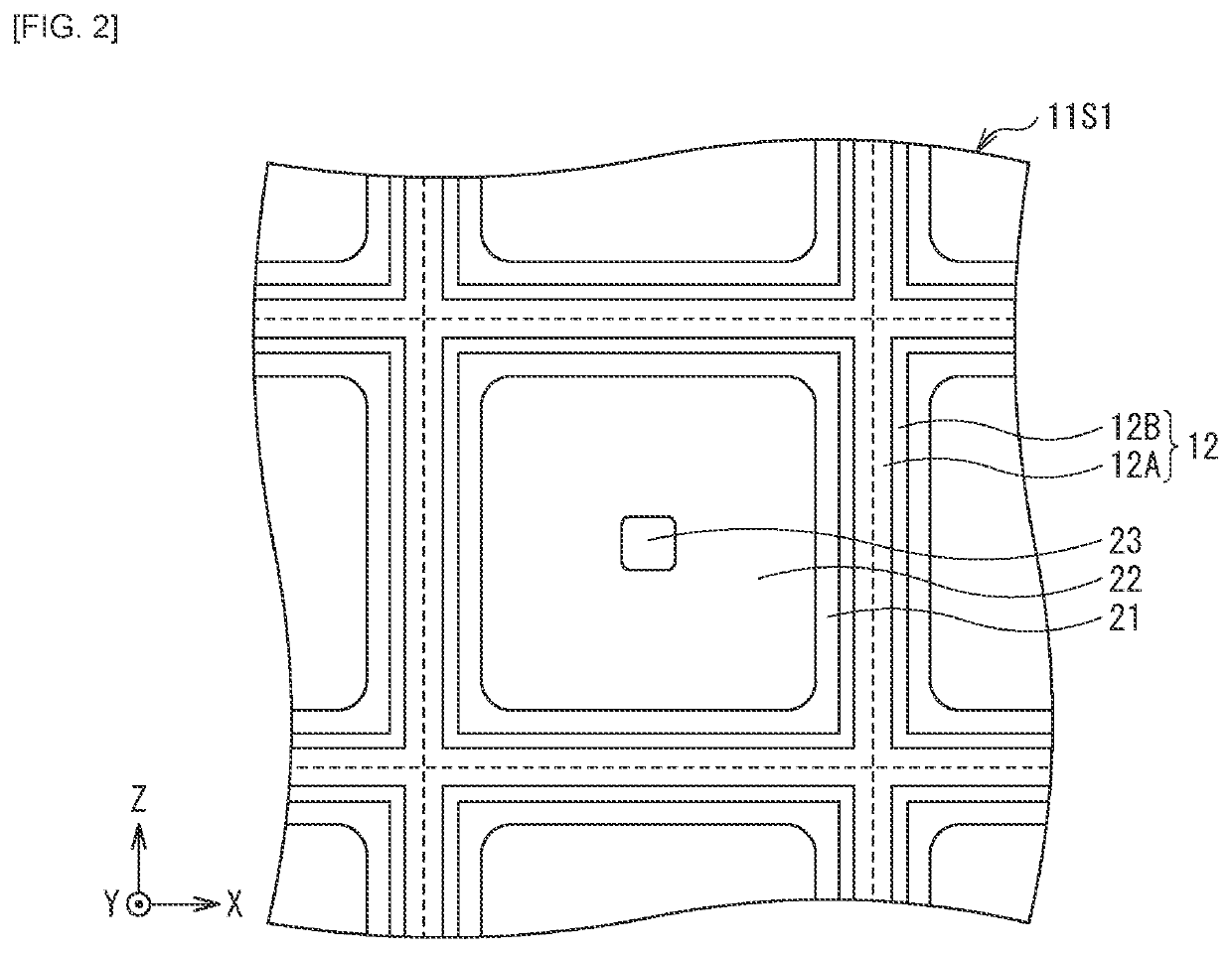
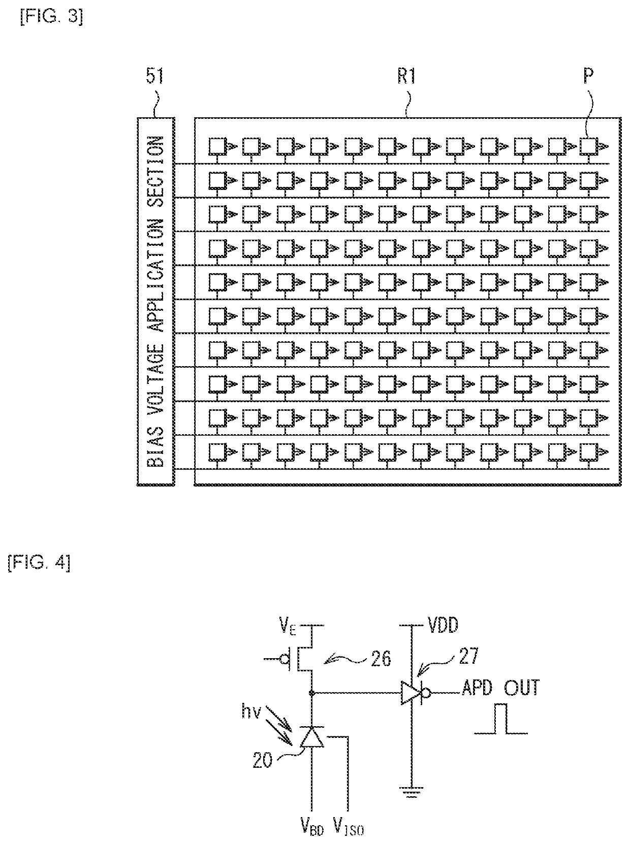
[0034]FIG. 1 schematically illustrates an example of a cross-sectional configuration of a sensor chip (a sensor chip 1) according to an embodiment of the present disclosure. FIG. 2 schematically illustrates an example of a planar configuration of a pixel array section R1 of the sensor chip 1 illustrated in FIG. 1. FIG. 3 is a block diagram illustrating a configuration of the sensor chip 1 illustrated in FIG. 1, and FIG. 4 illustrates an example of an equivalent circuit of a pixel P of the sensor chip 1 illustrated in FIG. 1. The sensor chip 1 is configured to be applied to, for example, a distance image sensor (a distance measurement device), an image sensor, or the like that performs distance measurements by a ToF (Time-of-Flight) method.

[0035]The sensor chip 1 includes, for example, the pixel array section R1 in which a plurality of pixels P is arranged in an array, and a peripheral section R2 provided around the pixel array section R1. The plurality of pixels P each ...

modification examples

2. Modification Examples

2-1. Modification Example 1

[0071]FIG. 8 schematically illustrates an example of a cross-sectional configuration of a sensor chip (a sensor chip 2) according to Modification Example 1 of the present disclosure. FIG. 9 schematically illustrates an example of a cross-sectional configuration at another position in the sensor chip 2. FIG. 10A schematically illustrates a planar configuration taken along line I-I′ illustrated in FIGS. 8 and 9, and FIG. 10B schematically illustrates a planar configuration taken along line II-II′ illustrated in FIGS. 8 and 9. It is to be noted that FIG. 8 illustrates a cross section taken along line A-A′ illustrated in FIGS. 10A and 10B, and FIG. 9 illustrates a cross section taken along line B-B′ illustrated in FIGS. 10A and 10B. Similarly to the sensor chip 1 of the foregoing embodiment, the sensor chip 2 is configured to be applied to, for example, a distance image sensor (a distance measurement device) that performs distance measu...

modification example 2

2-2. Modification Example 2

[0077]FIG. 13 schematically illustrates an example of a cross-sectional configuration of a sensor chip (a sensor chip 3) according to Modification Example 2 of the present disclosure. Similarly to the sensor chip 1 of the foregoing embodiment, the sensor chip 3 is configured to be applied to, for example, a distance image sensor (a distance measurement device) that performs distance measurements by the ToF method. The sensor chip 3 of the present modification example is different from the foregoing embodiment in that a wiring line is coupled to the pixel separation section 12.

[0078]A wiring line 15C, pad sections 16C and 34C, and a pad electrode 35C are electrically coupled to the pixel separation section 12 of the present modification example via the contact electrodes 17, 18, and 36, and it is possible to apply a voltage to the pixel separation section 12 independently of the anode (the contact electrode 17 in the peripheral section R2) and the cathode (...


PUM


Abstract

A sensor chip of an embodiment of the present disclosure includes: a semiconductor substrate including a pixel array section in which a plurality of pixels is arranged in an array; a light receiving element provided in the semiconductor substrate for each of the pixels and including a multiplier region in which avalanche multiplication of carriers is caused by a high electric field region; and a first pixel separation section provided between the pixels, the first pixel separation section extending from one surface of the semiconductor substrate toward another surface thereof opposed to the one surface, and having a bottom in the semiconductor substrate.

Description

TECHNICAL FIELD[0001]The present disclosure relates to a sensor chip using, for example, an avalanche photodiode, and a distance measurement device including the sensor chip.BACKGROUND ART[0002]In a distance measurement image sensor (a distance measurement device) that uses a single photon avalanche diode (SPAD), light emission in a high electric field region in a pixel at the time of multiplication of carriers can cause a photon to enter an adjacent pixel, thereby causing a signal to be unintentionally detected in the adjacent pixel. To cope with this, for example, PLT 1 discloses a sensor chip in which an inter-pixel separation section that physically separates a pixel from another adjacent pixel is provided in a semiconductor substrate in which an avalanche photodiode element is formed.CITATION LISTPatent Literature[0003]PTL 1: Japanese Unexamined Patent Application Publication No. 2018-88488SUMMARY OF THE INVENTION[0004]Meanwhile, a reduction in pixel size is demanded of a senso...

Claims


Application Information

Patent Timeline
IPC IPC(8): H01L27/146H01L31/107
CPCH01L27/1463H01L31/107H01L27/14643H01L27/146H01L31/02027
Inventor MATSUMOTOKITANO, YOSHIAKITAKATSUKA, YUSUKE
Owner SONY SEMICON SOLUTIONS CORP
Why Eureka
Try Eureka