

Method of forming thin film and method of modifying surface of thin film
- Summary
- Abstract
- Description
- Claims
- Application Information
AI Technical Summary
Benefits of technology
Problems solved by technology
Method used
Image

Examples
first embodiment
of Method of Forming Thin Film
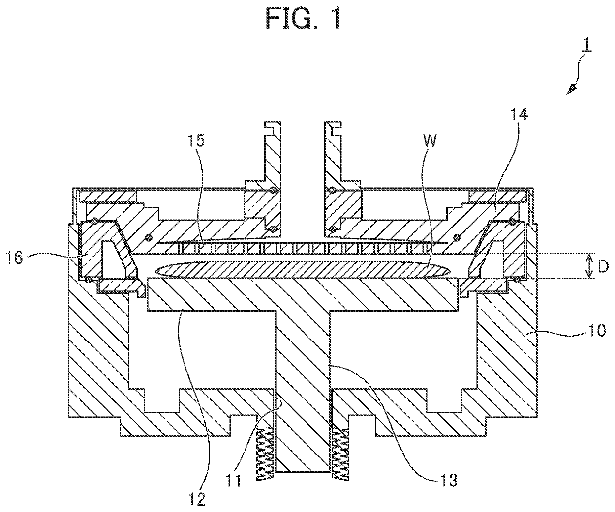
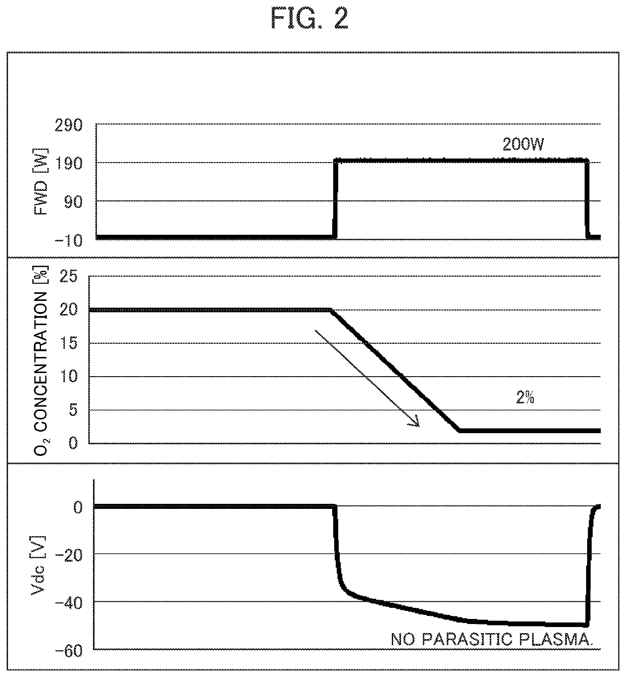
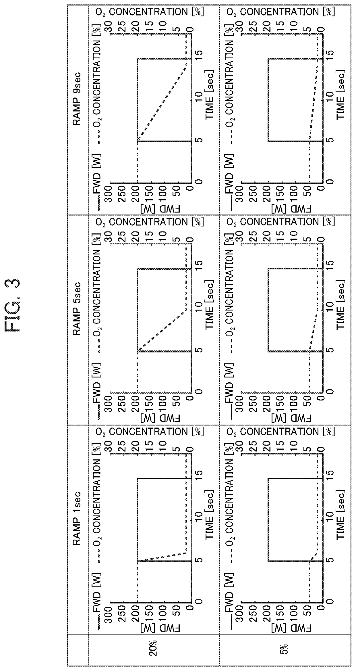
[0045]In a first embodiment of the method of forming a thin film according to this embodiment, a thin film is prepared on the substrate by the plasma-enhanced atomic layer deposition (PEALD) process. And when the reactant component (the gas component that is activated by the plasma generation) of the treatment gas is subjected to the plasma generation by applying the high-frequency power into the chamber, the first plasma generation condition in which high-frequency power of a second power level that is identical to that of the second plasma generation condition described below is applied while the treatment gas in which the concentration of the reactant component is the first concentration is supplied is changed to the second plasma generation condition by gradually decreasing the concentration of the reactant component to a second concentration from the first concentration while applying the high-frequency power of the second power level.
[0046][Substr...
second embodiment
of Method of Forming Thin Film
[0072]In a second embodiment of the method of forming a thin film according to this embodiment, the thin film is prepared on the substrate by the plasma-enhanced atomic layer deposition (PEALD) process. And in the plasma contact step, when the reactant component in the treatment gas is subjected to the plasma generation by applying the high-frequency power into the chamber, the first plasma generation condition in which the high-frequency power of the first power level is applied or the high-frequency power is not applied while the treatment gas in which the concentration of the reactant component is the second concentration that is identical to that of the second plasma generation condition described below is supplied is changed to the second plasma generation condition by gradually increasing the power level of the high-frequency power to the second power level while supplying the treatment gas of the second concentration.
[0073]In the method of formin...
third embodiment
of Method of Forming Thin Film
[0080]The methods of forming a thin film according to the first embodiment and the second embodiment may be combined with each other. In a third embodiment of the method of forming a thin film according to this embodiment, suppressing the abnormal electrical discharge by gradually decreasing the concentration of the reactant component in the first embodiment to the second concentration and suppressing the abnormal electrical discharge by gradually increasing the power level of the high-frequency power in the second embodiment to the second power level are combined. More specifically, in the plasma contact step, when the reactant component in the treatment gas is subjected to the plasma generation by applying the high-frequency power into the chamber, the first plasma generation condition in which the high-frequency power of the first power level is applied or the high-frequency power is not applied while the treatment gas in which the concentration of t...
PUM
| Property | Measurement | Unit |
|---|---|---|
| Power | aaaaa | aaaaa |
| Concentration | aaaaa | aaaaa |
Abstract
Description
Claims
Application Information