Light emitting device, optical device, and measurement device

Active Publication Date: 2021-08-26
FUJIFILM BUSINESS INNOVATION CORP
View PDF2 Cites 0 Cited by
  • Summary
  • Abstract
  • Description
  • Claims
  • Application Information

AI Technical Summary

Benefits of technology

[0004]Aspects of non-limiting embodiments of the present disclosure relate to the following circumstances. Three-dimensional shapes of targets may be measured based on so-called Time of Flight (ToF) using a

Problems solved by technology

However, aspects of the non-limiting embodiments are not required to address the advantages described above, an

Method used


Image

  • Light emitting device, optical device, and measurement device
  • Light emitting device, optical device, and measurement device
  • Light emitting device, optical device, and measurement device

Examples


Embodiment Construction

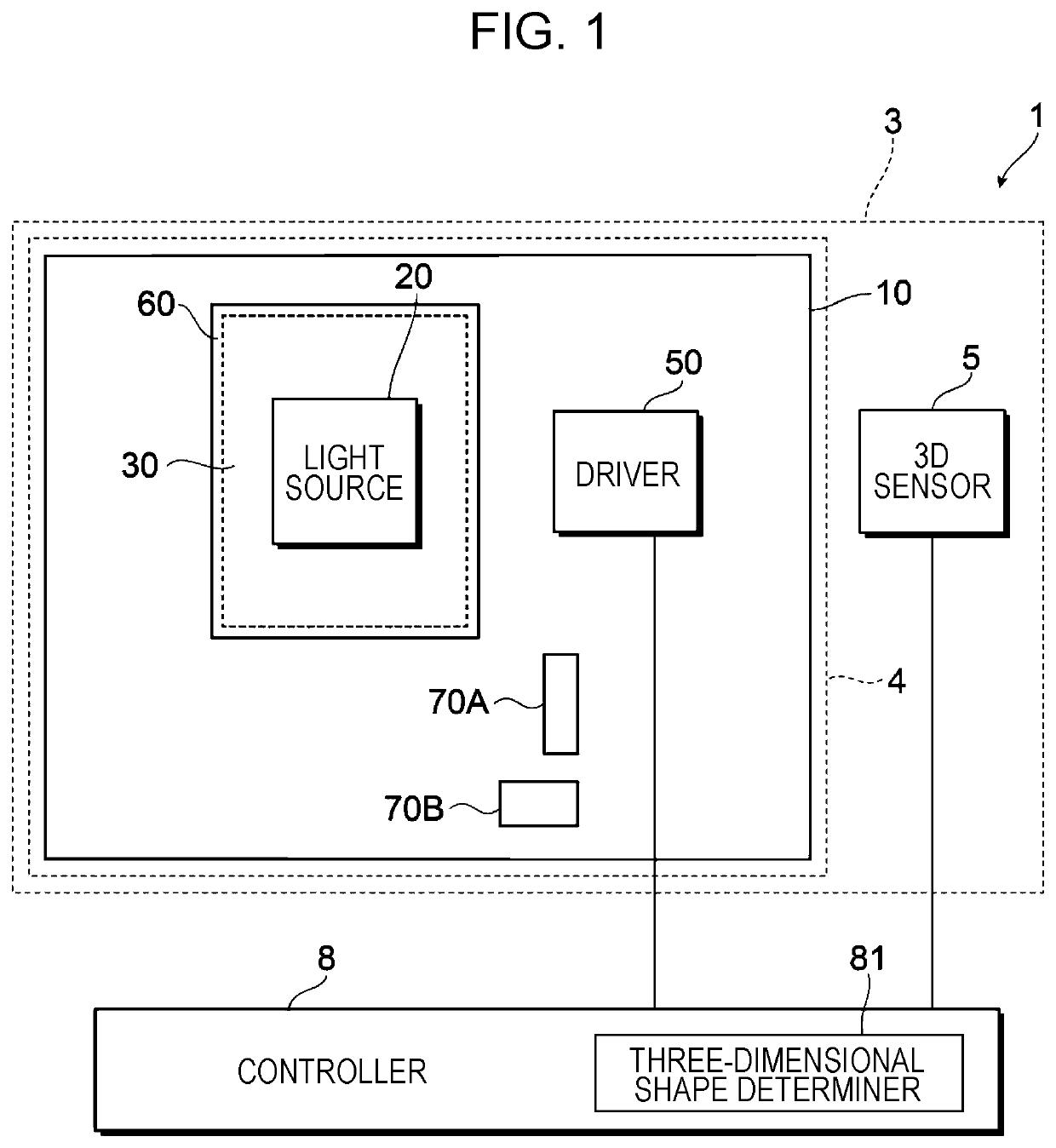
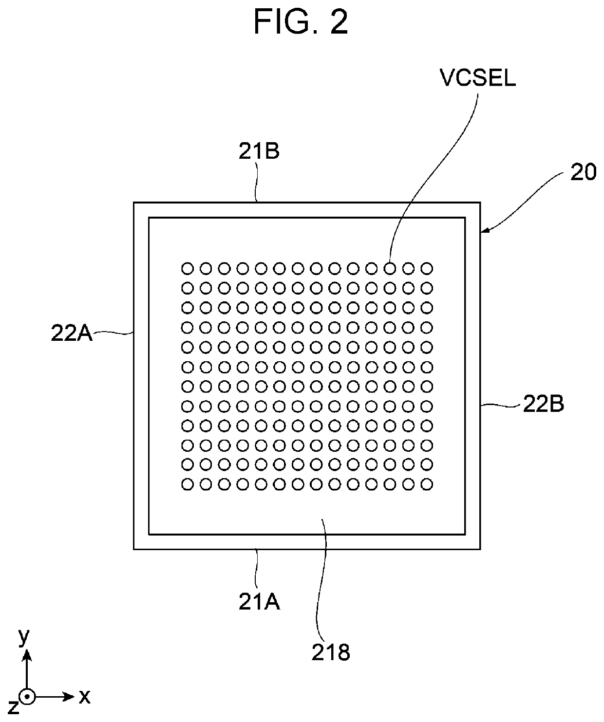
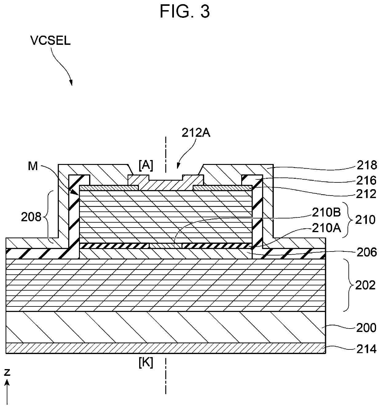
[0026]An exemplary embodiment of the present disclosure is described below in detail with reference to the accompanying drawings.

[0027]There is a measurement device that measures three-dimensional shapes of targets based on so-called Time of Flight (ToF) using a time of traveling light. In ToF, the three-dimensional shape of a target is determined by measuring a period from a timing when a light source of the measurement device emits light to a timing when the emitted light is reflected on the target and received by a three-dimensional sensor (hereinafter referred to as “3D sensor”) of the measurement device. The term “target” refers to an object subjected to measurement of its three-dimensional shape. The measurement of the three-dimensional shape may be referred to as “three-dimensional measurement”, “3D measurement”, or “3D sensing”.

[0028]For example, the measurement device is mounted on a portable information processing apparatus and is used for facial recognition of users who a...


PUM


Abstract

A light emitting device includes a wiring board having a first wiring layer and a second wiring layer adjacent to the first wiring layer via an insulating layer, and a laser having a cathode electrode and an anode electrode, mounted on the wiring board, and driven through low-side driving. The first wiring layer includes a cathode wire connected to the cathode electrode, an anode wire connected to the anode electrode, and a first reference potential wire connected to a reference potential. The second wiring layer includes a second reference potential wire connected to the reference potential. An area of an overlap between the second reference potential wire and the anode wire is larger than an area of an overlap between the second reference potential wire and the first reference potential wire.

Description

CROSS-REFERENCE TO RELATED APPLICATIONS[0001]This application is based on and claims priority under 35 USC 119 from Japanese Patent Application No. 2020-030317 filed Feb. 26, 2020.BACKGROUND(i) Technical Field[0002]The present disclosure relates to a light emitting device, an optical device, and a measurement device.(ii) Related Art[0003]Japanese Unexamined Patent Application Publication No. 2008-252129 describes a light emitting device including a light-transmissive ceramic substrate, a light emitting element mounted on the front face of the ceramic substrate, a wiring pattern for power supply to the light emitting element, and a metalized layer made of a metal having light reflectivity. The metalized layer is formed inside the ceramic substrate to reflect light emitted from the light emitting element.SUMMARY[0004]Aspects of non-limiting embodiments of the present disclosure relate to the following circumstances. Three-dimensional shapes of targets may be measured based on so-calle...

Claims


Application Information

Patent Timeline
IPC IPC(8): H01S5/042H01S5/02255
CPCH01S5/04256G01S17/894H01S5/02255H01S5/423G01B11/24H01S5/02208H01S5/02257H01S5/02345H01S5/0239H01S5/02469H01S5/02476H01S5/0428H01S5/06216H03K3/53G01S7/4815
Inventor IGUCHI, DAISUKESAKAI, KAZUHIRO
Owner FUJIFILM BUSINESS INNOVATION CORP
Why Eureka
Try Eureka