
Eureka
For R&D, Eureka makes reading and utilizing patents & technical documents easy.
Eureka AIR
Designed for self-driven R&D workflows. Generate viable solutions, solve complex R&D challenges, empower your innovation with AI.

Eureka Materials
Designed for material experts only. Revolutionize your material R&D, from search, analyze, to developing new materials.

TechResearch
Generate reliable direction feasibility study reports for your R&D in just a few steps.

TechSeek
Discover and master advanced knowledge NOW. Basics, ideas, possibilities, all at once.

TechMind
As an expert in R&D Theories, TechMind can generates customized viable solutions instantly.

TechRisk
Analyze your overall solution with one click, know your potential R&D risks in advance.

TechMonitor
Get weekly tech updates, stay abreast of the latest tech innovations and key insights.
Multi-layer ceramic electronic component, circuit board, and method of producing a multi-layer ceramic electronic component
- Summary
- Abstract
- Description
- Claims
- Application Information
AI Technical Summary
Benefits of technology
Problems solved by technology
Method used
Image

Examples
Embodiment Construction
[0039]Hereinafter, embodiments of the present disclosure will be described with reference to the drawings.
[0040]In the figures, an X axis, a Y axis, and a Z axis orthogonal to one another are shown as appropriate. The X axis, the Y axis, and the Z axis are common in all figures.
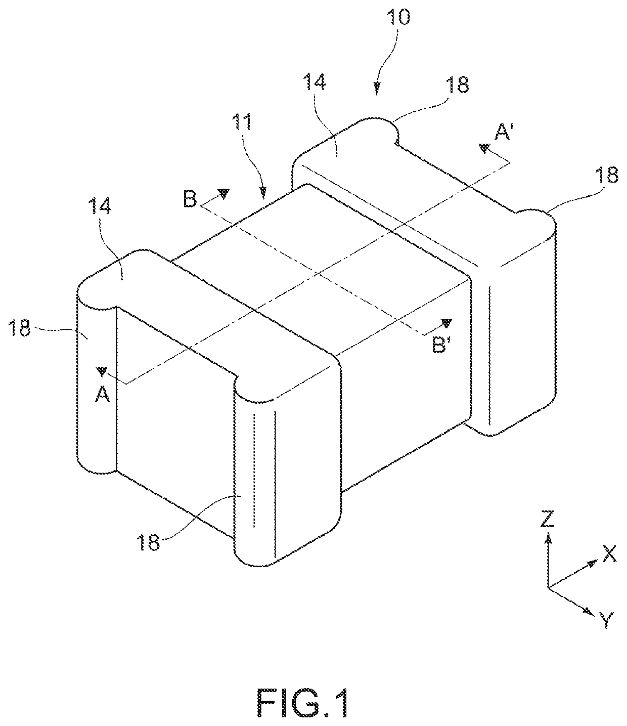
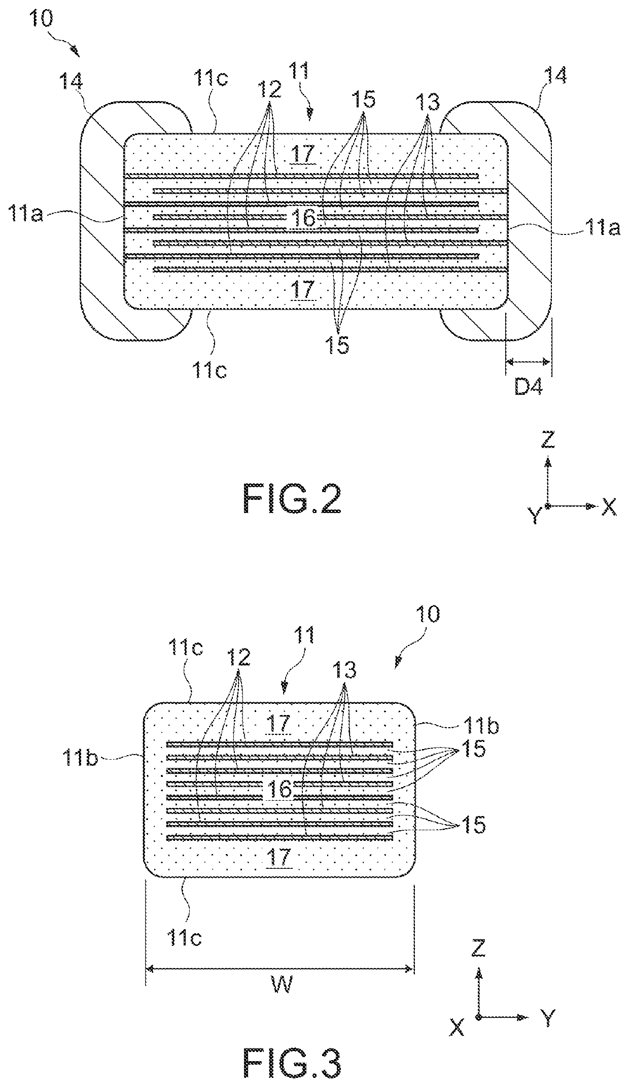
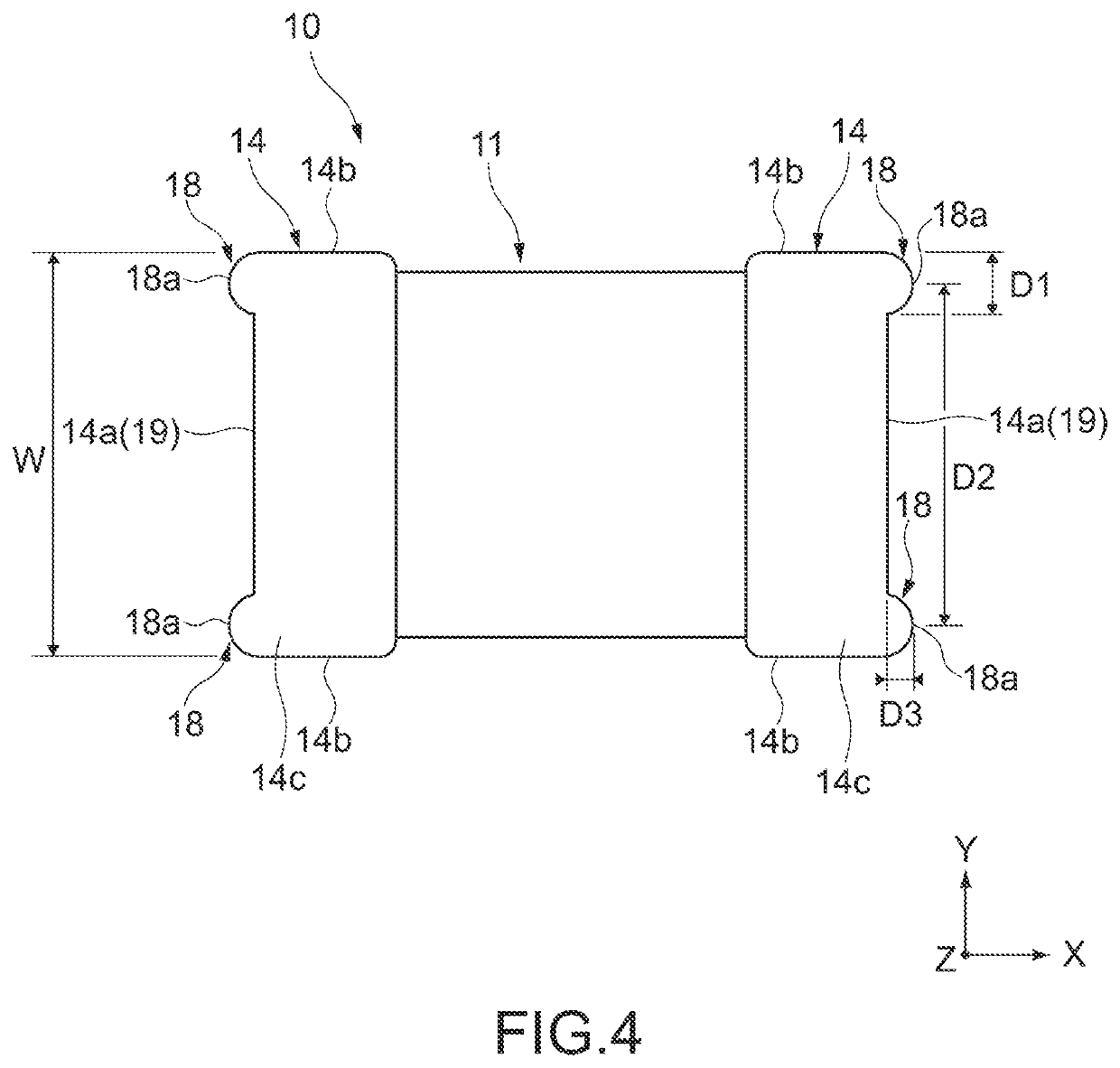
1. Configuration of Multi-Layer Ceramic Capacitor 10
[0041]FIGS. 1 to 3 each show a multi-layer ceramic capacitor 10 according to an embodiment of the present disclosure. FIG. 1 is a perspective view of the multi-layer ceramic capacitor 10. FIG. 2 is a cross-sectional view of the multi-layer ceramic capacitor 10 taken along the A-A′ line in FIG. 1. FIG. 3 is a cross-sectional view of the multi-layer ceramic capacitor 10 taken along the B-B′ line in FIG. 1.
[0042]The multi-layer ceramic capacitor 10 includes a ceramic body 11 and external electrodes 14.
[0043]The ceramic body 11 has two end surfaces 11a facing each other in the X-axis direction, two side surfaces 11b facing each other in the Y-axis direction, and...
PUM
| Property | Measurement | Unit |
|---|---|---|
| Length | aaaaa | aaaaa |
| Length | aaaaa | aaaaa |
| Length | aaaaa | aaaaa |
Abstract
Description
Claims
Application Information
 - R&D Engineer
- R&D Manager
- IP Professional
- Industry Leading Data Capabilities
- Powerful AI technology
- Patent DNA Extraction
Browse by: Latest US Patents, China's latest patents, Technical Efficacy Thesaurus, Application Domain, Technology Topic, Popular Technical Reports.
© 2024 PatSnap. All rights reserved.Legal|Privacy policy|Modern Slavery Act Transparency Statement|Sitemap|About US| Contact US: help@patsnap.com