Active matrix organic light emitting diode (amoled) display panel

Inactive Publication Date: 2021-11-04
WUHAN CHINA STAR OPTOELECTRONICS SEMICON DISPLAY TECH CO LTD
View PDF0 Cites 4 Cited by
  • Summary
  • Abstract
  • Description
  • Claims
  • Application Information

AI Technical Summary

Benefits of technology

[0028]The beneficial effect of this invention is: comparing with an AMOLED display panel of the prior art, in the AMOLED display panel of the application, the cathodes and the sensing electrodes are formed in the cathode layer by a patterned process, adjacent second sensing electrodes defined in the second electrode rows are connected with each other by the cathode layer, adjacent first sensing electrodes defined in the first electrode rows are connected by the first conductive bridges, adjacent cathodes are connected with each other by the second conductive

Problems solved by technology

Both types of fingerprint recognition have certain deficiencies, the front-fingerp

Method used


Image

  • Active matrix organic light emitting diode (amoled) display panel
  • Active matrix organic light emitting diode (amoled) display panel
  • Active matrix organic light emitting diode (amoled) display panel

Examples


Example

[0036]The description of following embodiment, with reference to the accompanying drawings, is used to exemplify specific embodiments which may be carried out in the present disclosure. Directional terms mentioned in the present disclosure, such as “top”, “bottom”, “front”, “back”, “left”, “right”, “inside”, “outside”, “side”, etc., are only used with reference to the orientation of the accompanying drawings. Therefore, the used directional terms are intended to illustrate, but not to limit, the present disclosure. In the drawings, the components having similar structures are denoted by same numerals.

[0037]The present disclosure is directed to a technology problem of a limited screen-to-body ratio caused by fingerprint identification units and the display area separated with each other of the prior art. The present disclosure can solve the above defects.

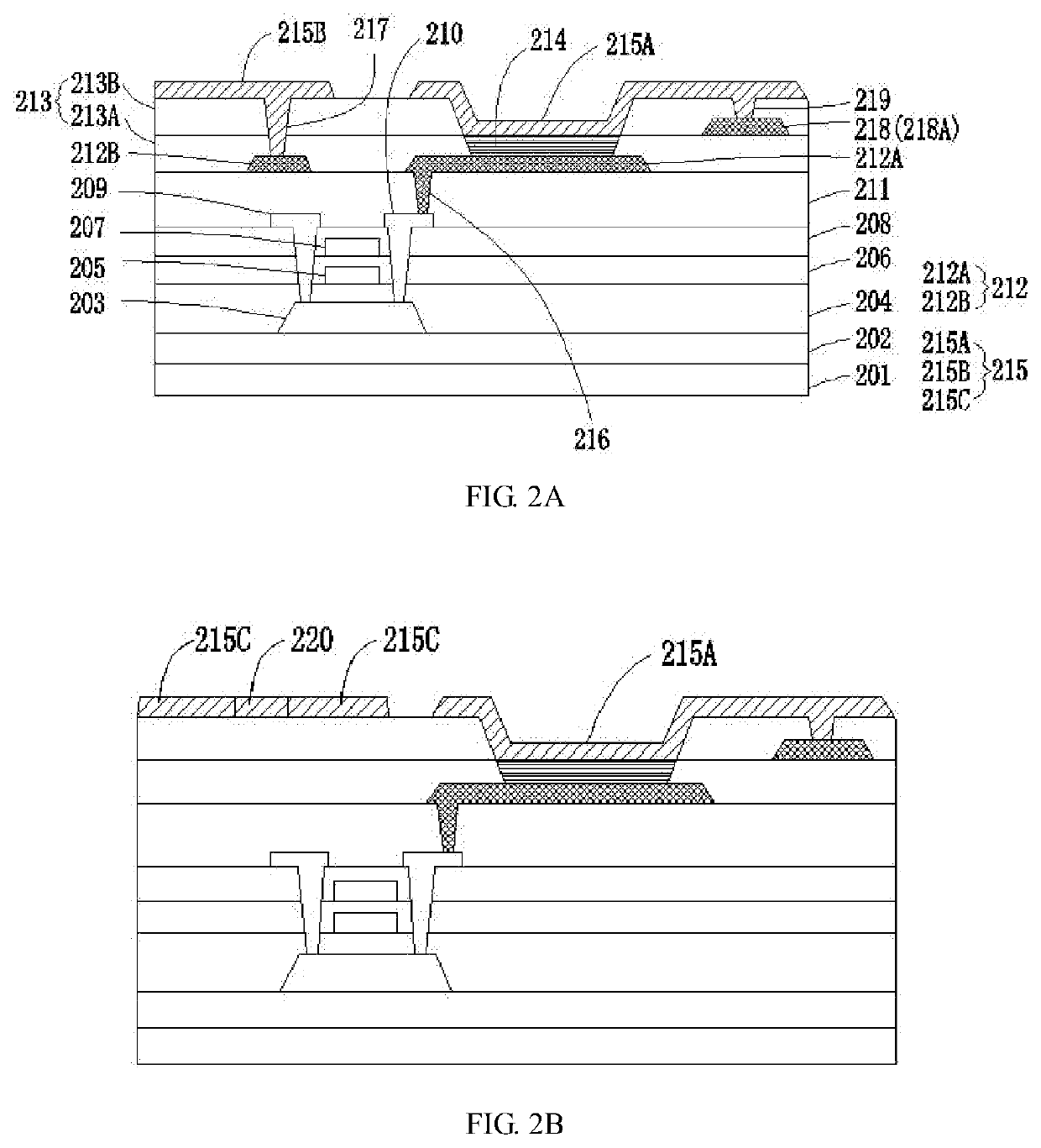
[0038]Referring to FIG. 2A, FIG. 2A is a schematic view of a film layer structure of an AMOLED display panel along a direction of a...


PUM


Abstract

The present disclosure provides an active matrix organic light emitting diode (AMOLED) display panel. The AMOLED display panel includes a base substrate and an anode layer, a pixel defining layer, a light emitting layer, a second metal layer, and a cathode layer formed on the base substrate. The cathode layer includes a plurality of cathodes and a plurality of sensing electrodes electrically insulated from the cathodes. A plurality of first electrode rows and a plurality of second electrode rows are formed by the sensing electrodes and insulated from each other. The sensing electrodes of the first electrode rows are used to couple to the sensing electrodes of the second electrode rows to make capacitors.

Description

CROSS REFERENCE TO RELATED APPLICATION[0001]This application claims the priority of International Application No. PCT / CN2018 / 107010, filed on Sep. 21, 2018, which claims priority to Chinese Application No. 201811022187.X, filed on Sep. 4, 2018. The entire disclosures of each of the above applications are incorporated herein by reference.BACKGROUND OF INVENTIONField of Invention[0002]The present invention relates to a display technology field, and particularly to an active-matrix organic light emitting diode (AMOLED) display panel.Description of Prior Art[0003]Active-matrix organic light emitting diodes, referred to as AMOLEDs, or active matrix organic light emitting diode panels. At present, there are two types of fingerprint identification schemes on the market. One is a front fingerprint recognition integrated in a home button, and the other one is a rear fingerprint identification of the individual fingerprint recognition area on a back of the case. Both types of fingerprint reco...

Claims


Application Information

Patent Timeline
IPC IPC(8): H01L51/52H01L27/32G06K9/00G06F3/041G06F3/044
CPCH01L51/5215H01L51/5225H01L27/3246G06F2203/04111G06K9/0002G06F3/0412G06F3/0446H01L27/323G06V40/1306H10K59/40H10K59/131H10K50/82G06V40/1318H10K59/1315H10K50/816H10K50/822H10K59/122
Inventor ZHENG, YUANYEN, CHIHCHENG
Owner WUHAN CHINA STAR OPTOELECTRONICS SEMICON DISPLAY TECH CO LTD
Why Eureka
Try Eureka