Integrated circuit testing for integrated circuits with antennas

a technology of integrated circuits and integrated circuits, which is applied in the direction of measuring devices, protective materials radiating elements, instruments, etc., can solve the problems of high cost, special problems, and the difficulty of customizing the test method,

Active Publication Date: 2021-11-18
JOHNSTECH INT
View PDF0 Cites 4 Cited by
  • Summary
  • Abstract
  • Description
  • Claims
  • Application Information

AI Technical Summary

Benefits of technology

[0009]Also disclosed is a method of constructing the enclosure of a radio absorptive material to prevent RF sig

Problems solved by technology

Chips (such as semiconductor devices and/or integrated circuits) which can transmit or receive radio frequency (RF) signals need to be tested like other chips but they present special problems.
For example, the placement of the transmit antenna on different chips may not be consistent and thus receiving and testing the signal strength may require expensive and complicated custom set up to transition from testing one chip to testing a different chip.
Antennas transmit po

Method used


Image

  • Integrated circuit testing for integrated circuits with antennas
  • Integrated circuit testing for integrated circuits with antennas
  • Integrated circuit testing for integrated circuits with antennas

Examples


Embodiment Construction

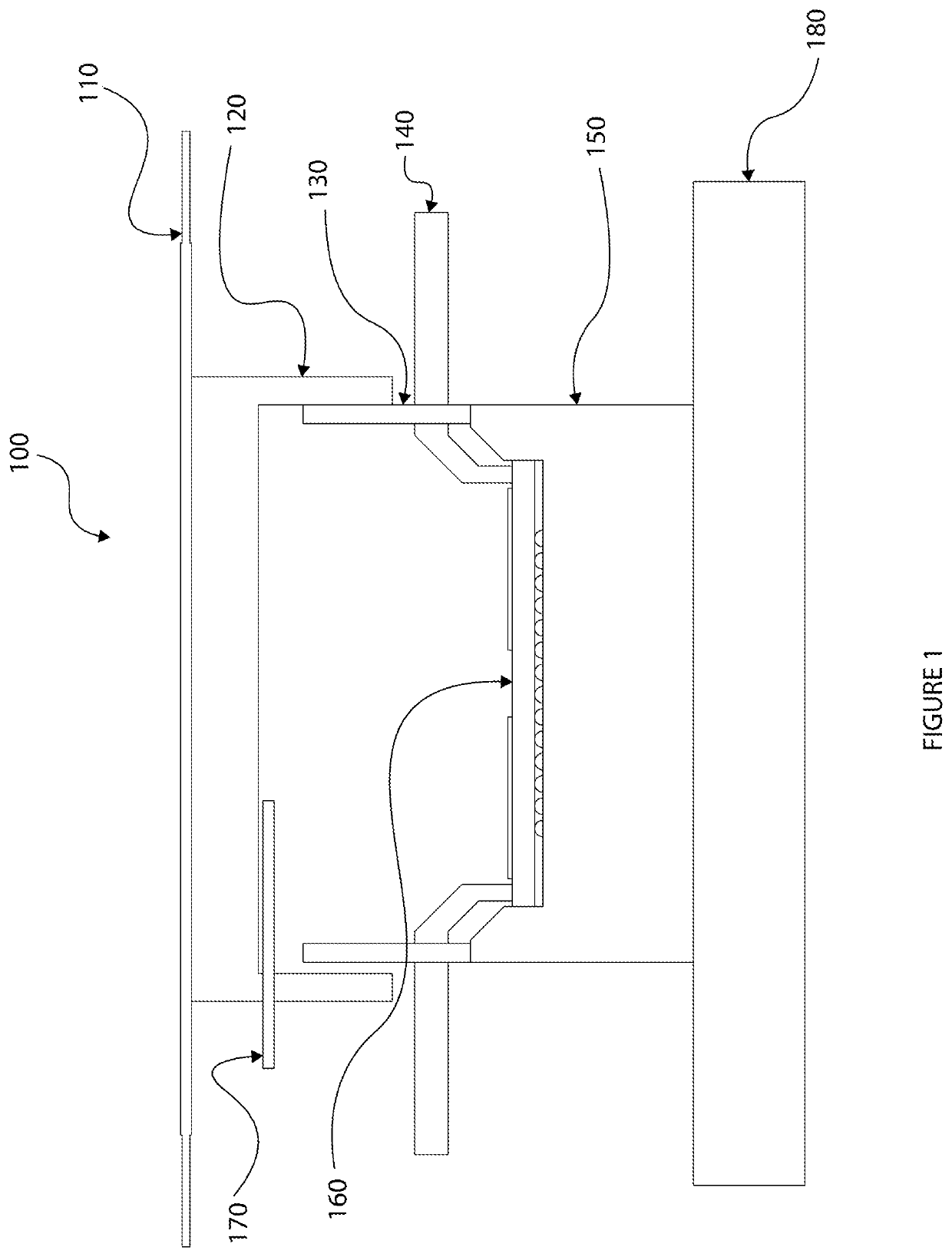
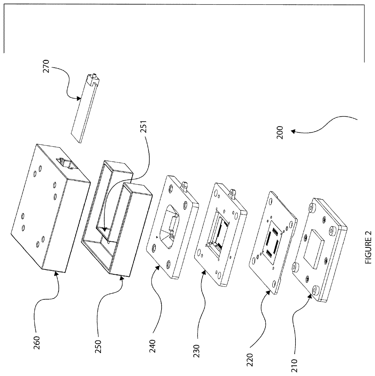
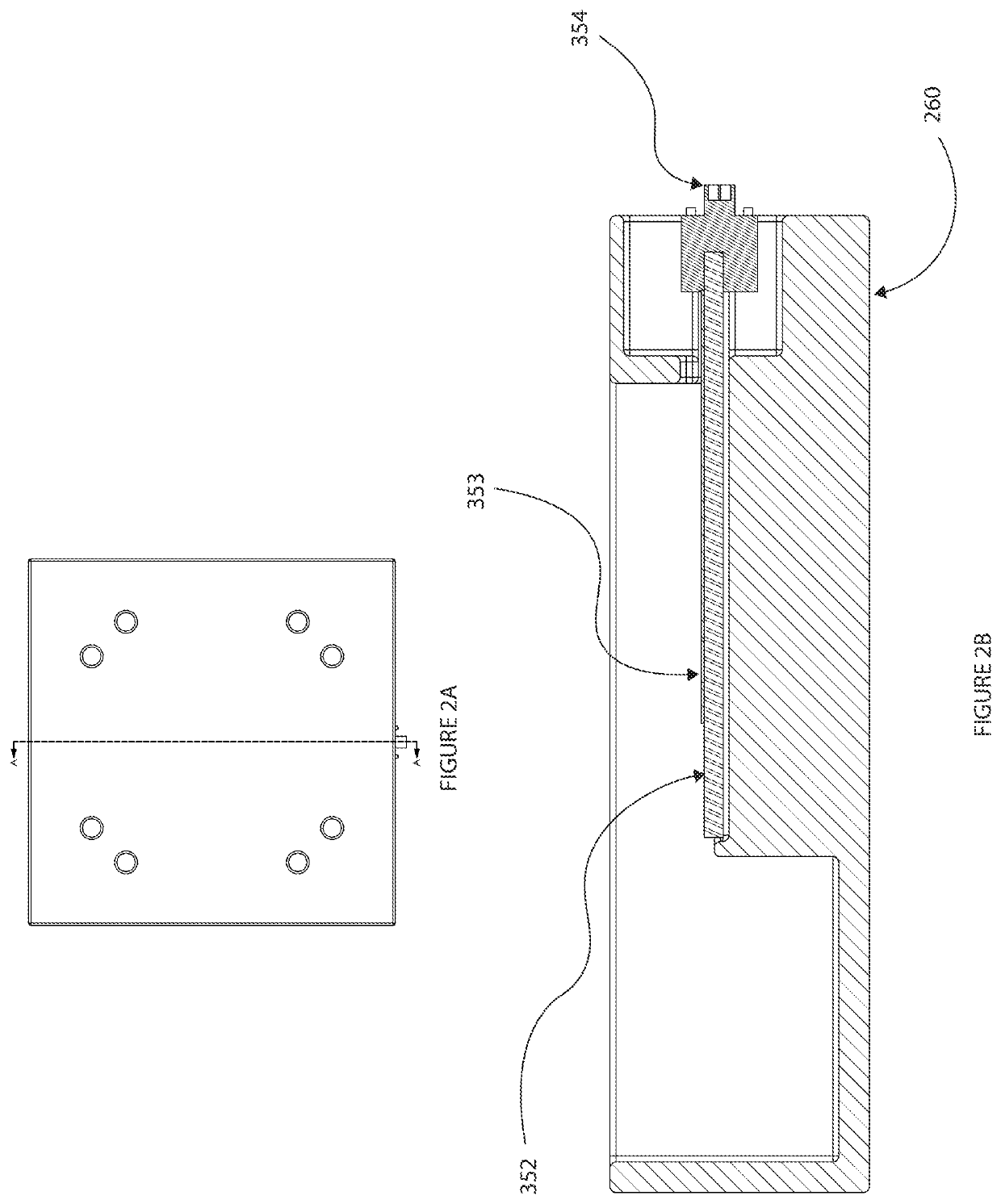
[0025]Some mission critical AiP (antenna in package) chips (such as semiconductor devices and / or integrated circuits (ICs)) may require extensive testing in a chamber (enclosure) because of regulatory requirements. Typically the AiP chip manufacturers may perform rigorous testing at wafer level and perform minimal testing at final OTA test to determine if antenna installation has caused chip damage. The embodiments disclosed herein can facilitate the final OTA testing in an expedient manner in an RF chamber which can save time and reduce the cost of testing.

[0026]Instead of using actual antenna patterns which typically take a long period of time to measure accurately and require large spaces to get measured results in far field of the antenna signals, embodiments disclosed herein are geared towards a final OTA testing where the performance of the RF signals of an antenna is compared to an actual “golden” unit (a unit known to have the exact desired characteristics) or to units that ...


PUM


Abstract

A testing system and method for testing integrated circuits with radio frequency (RF) antennas is disclosed. The system includes an alignment plate for receiving a device under test (DUT) having an RF transmitting antenna, an enclosure surrounding but separated from the transmitting antenna, a receiving antenna in a telescopic enclosure, and a conversion circuit connected to the receiving antenna. The conversion circuit is configured to convert an RF output from the DUT to a direct current (DC) voltage. The DC voltage is used as a proxy for the RF output to test the DUT. When testing chips with RF ports, the chip or ports are surrounded by the enclosure which is non-radio reflective and includes antennas for receiving RF outputs disbursed around the enclosure, or a single antenna. If multiple receiving antennas are used, sequential testing can also detect directional transmission patterns to confirm that the direction is correctly calibrated.

Description

CROSS REFERENCE AND INCORPORATION BY REFERENCE[0001]Priority is claimed from the following applications which are also hereby incorporated by reference in their entirely: U.S. Provisional Application No. 62 / 846,842 filed on 13 May 2019 of same title, and U.S. provisional application Ser. No. 62 / 988,028 filed on 11 Mar. 2020 of same title.TECHNICAL FIELD[0002]This disclosure relates generally to the field of testing semiconductor device(s) and / or integrated circuit(s). More specifically, the disclosure relates to systems and methods for testing semiconductor device(s) and / or integrated circuit(s) with antenna or with antennas being mounted on the top or on the side(s) of the semiconductor device(s) and / or the integrated circuit(s) in a package.BACKGROUND[0003]Chips (such as semiconductor devices and / or integrated circuits) which can transmit or receive radio frequency (RF) signals need to be tested like other chips but they present special problems. For example, the placement of the ...

Claims


Application Information

Patent Timeline
IPC IPC(8): G01R31/28G01R31/319H01Q1/22H01Q1/40
CPCG01R31/2822H01Q1/405H01Q1/2283G01R31/31905H01Q3/267G01R31/2896G01R29/105G01R1/045
Inventor SHERRY, JEFFREY
Owner JOHNSTECH INT
Why Eureka
Try Eureka